Lead pin for package substrate

a technology of lead pins and substrates, which is applied in the direction of conductors, semiconductor devices, semiconductor/solid-state device details, etc., can solve the problems of lead pin inclination, high cost, and high cost, so as to prevent the pollution of the connection pin, increase bonding efficiency, and increase the contact area

Inactive Publication Date: 2011-03-24
SAMSUNG ELECTRO MECHANICS CO LTD
View PDF6 Cites 16 Cited by
  • Summary
  • Abstract
  • Description
  • Claims
  • Application Information

AI Technical Summary

Benefits of technology

An aspect of the present invention provides a lead pin for a package substrate that prevents the pollution of a connection pin due to a solder paste and increases bonding efficiency by increasing a contact area between a head part and the solder paste.
According to an aspect of the present invention, there is provided a lead pin for a package substrate including: a connection pin being inserted into a hole formed in an external substrate; a head part formed on one end of the connection pin; and a barrier part formed on one surface of the head part in order to block the path of a solder paste so that the solder paste is prevented from flowing so as to cover the upper portion of the head part when the head part is mounted on the package substrate.
According to another aspect of the present invention, there is provided a lead pin for a semiconductor package including: a connection pin being inserted into a hole formed in an external substrate; a head part including a flange part formed on one end of the connection pin and a plane part formed on the upper portion of the flange part and having a flat shaped end; and a barrier part formed on one surface of the head part in order to block the path of a solder paste so that the solder paste is prevented from flowing so as to cover the upper portion of the head part when the head part is mounted on the package substrate.
Meanwhile, according to another aspect of the present invention, there is provided a semiconductor package including: a substrate part having one surface on which a pad part is formed; and a lead pin including: a connection pin being inserted into a hole formed in an external substrate; a head part including a flange part formed on one end of the connection pin and a plane part formed on the upper portion of the flange part and having a flat shaped end; and a barrier part formed on one surface of the head part in order to block the path of a solder paste so that the solder paste is prevented from flowing so as to cover the upper portion of the head part when the head part is mounted on the package substrate, the lead pin being electrically connected to the pad part.
According to another aspect of the present invention, there is provided a lead pin for a semiconductor package including: a connection pin being inserted into a hole formed in an external substrate; a head part including a flange part formed on one end of the connection pin and a projection part formed on the upper portion of the flange part and having a multi-layer shape; and a barrier part formed on one surface of the head part in order to block the path of a solder paste so that the solder paste is prevented from flowing so as to cover the upper portion of the head part when the head part is mounted on the package substrate.
According to another aspect of the present invention, there is provided a semiconductor package including: a substrate part having one surface on which a pad part is formed; and a lead pin including: a connection pin being inserted into a hole formed in an external substrate; a head part including a flange part formed on one end of the connection pin and a projection part formed on the upper portion of the flange part and having a multi-layer shape; and a barrier part formed on one surface of the head part in order to block the path of a solder paste so that the solder paste is prevented from flowing so as to cover the upper portion of the head part when the head part is mounted on the, package substrate, the lead pin being electrically connected to the pad part.

Problems solved by technology

The T-type lead pin has gradually become widespread due to a limitation of the available area for the circuit configuration of the package substrate as compared to the pin insert type.
As the use of lead has been recently limited in consideration of environmental effects due to soldering, a solder (Sn—Ag—Cu, and Sn—Sb) not using lead has been used, such that the melting temperature of the solder is increased.
At this time, as the melting temperature of the soldering is high, solder for connecting lead pins that support lead pins is melted by reflow heat during a reflow process for mounting an IC chip on a package substrate, thereby causing an inclination of the lead pins.
In addition, defects frequently occur, such as in the case that solder paste overflows toward the upper portions of the lead pins during the reflow process so as to be spread to connection pins and the like.

Method used


Image

  • Lead pin for package substrate
  • Lead pin for package substrate
  • Lead pin for package substrate

Examples


second embodiment

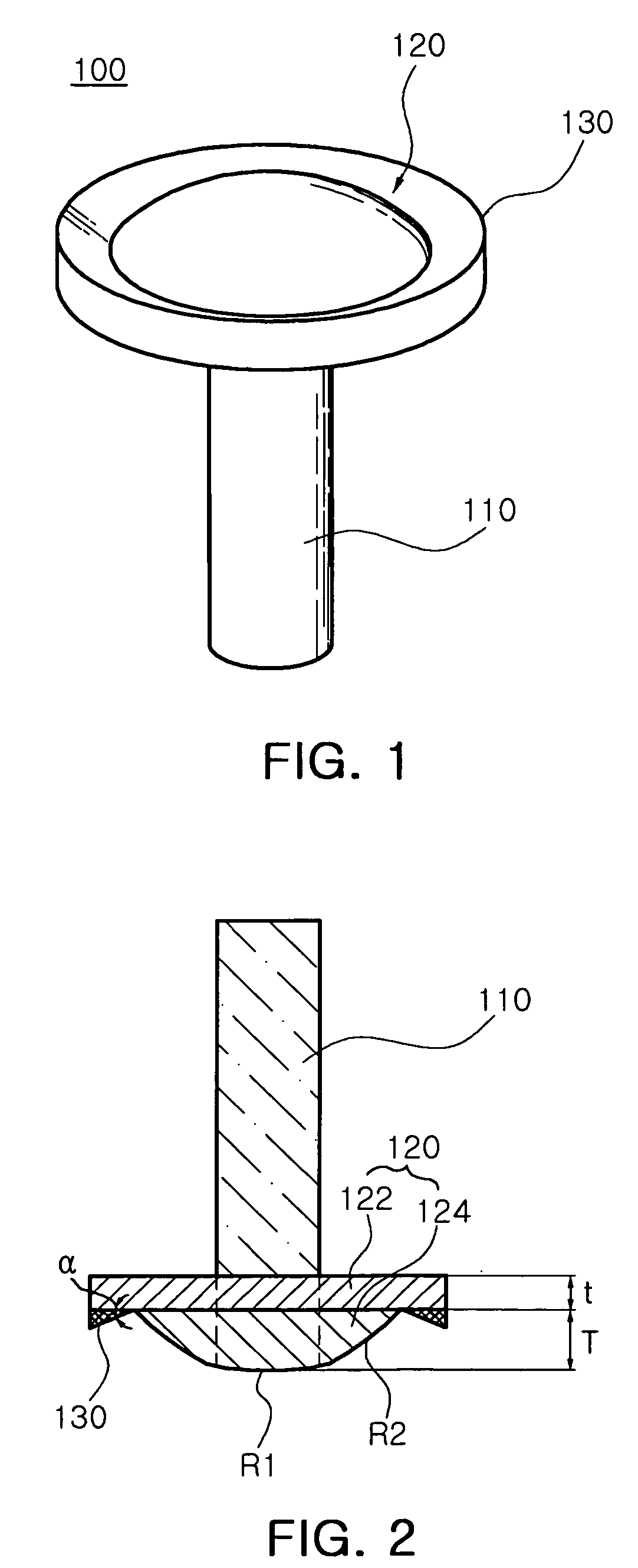
FIG. 6 is a cross-sectional view explaining a lead pin for a package substrate according to the present invention.

Referring to FIG. 6, the lead pin for the package substrate may include a connection pin 210, a head part 220, and a barrier part 230.

At this time, the connection pin 210 and the head part 220 are substantially the same as those shown in the previous embodiment, such that the detailed description thereof may be omitted.

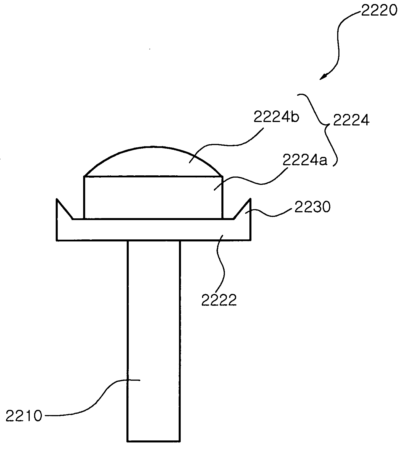
The barrier part 230 is formed so as to be positioned on a side surface of a flange 222, wherein it may have a shape projected from the side surface.

Also, the barrier part 230 may be projected, in a tapered shape, to the one edge of the flange part 222. Therefore, the barrier part 230 allows the length of the flange part 222 to be extended in the edge side.

Therefore, the lead pin for the package substrate according to the present embodiment includes the barrier part 230 that blocks the path of the solder paste so as to prevent the solder paste from flowing...

third embodiment

FIG. 7 is a side cross-sectional view explaining a semiconductor package according to the present invention, and FIG. 8 is a partial cross-sectional view explaining a state in which the lead pin of FIG. 7 is mounted on a substrate.

Referring to FIGS. 7 and 8, the semiconductor package 10 may include a substrate part 20 and a lead pin 1100.

A semiconductor chip 30 is electrically connected to the surface of the substrate part 20, wherein the substrate part 20 may use an organic substrate or a ceramic substrate such as a low temperature co-fired ceramic (LTCC).

In addition, a pad part 22 that is electrically connected to the lead pin 1100 may be formed on the bottom surface of the substrate part 20 and a photoresist layer 50 may be provided around the pad part 22. Also, the substrate part 20 may be manufactured in a plurality of layers, and circuit patterns that electrically connect the plurality of layers may be formed therein.

Therefore, the semiconductor chip 30 is mounted so as to be ...

fourth embodiment

FIGS. 11 and 12 are cross-sectional views explaining a plane part and a barrier part of a lead pin according to the present invention.

Referring to FIG. 11, the lead pin may include a connection pin 1210, a head part 1220, and a barrier part 1230.

Herein, the connection pin 1210 and the barrier part 1230 according to the present embodiment are substantially the same as those shown in the previous embodiment, such that the detailed description thereof may be omitted.

At this time, the barrier part 1230 and a plane part 1224 may be spaced apart from each other on a flange part 1222. At this time, the barrier part 1230 and the plane part 1224 may be connected to each other and the barrier part 1230 and the plane part 1224 may be spaced apart from each other by processing portions adjacent to the plane part 1224.

Referring to FIG. 12, it may be appreciated that a portion in which the plane part 1324 and the barrier part 1330 contact each other is formed so as to have a curved surface. There...


PUM

PropertyMeasurementUnit
angleaaaaaaaaaa
inclined angleaaaaaaaaaa
diameteraaaaaaaaaa

Abstract

There is provided a lead pin for a package substrate including: a connection pin being inserted into a hole formed in an external substrate; a head part formed on one end of the connection pin; and a barrier part formed on one surface of the head part in order to block the path of a solder paste so that the solder paste is prevented from flowing so as to cover the upper portion of the head part when the head part is mounted on the package substrate.

Description

CROSS-REFERENCE TO RELATED APPLICATIONSThis application claims the priority of Korean Patent Application Nos. 10-2009-0089707 filed on Sep. 22, 2009, 10-2009-0123275 filed on Dec. 11, 2009, and 10-2009-0125087 filed on Dec. 15, 2009, in the Korean Intellectual Property Office, the disclosures of which are incorporated herein by reference.BACKGROUND OF THE INVENTION1. Field of the InventionThe present invention relates to a lead pin for a package substrate, and more particularly, to a lead pin for a package substrate that connects a package substrate on which an integrated circuit is mounted to a main board.2. Description of the Related ArtWith the development of electronics industry, semiconductor packages in various types have been manufactured. Recently, as the wiring density of a semiconductor package has been increased, a semiconductor package substrate of a Pin Grid Array (PGA) type in which a plurality of T-type lead pins are mounted has been widely used as a substrate that co...

Claims


Application Information

Patent Timeline
Patent Type & Authority Applications(United States)
IPC IPC(8): H01L23/498H01B5/00
CPCH01L23/49811H01L2924/09701H01L23/49805H01L2924/0002H01L2924/00
Inventor LEE, KI TAEKOH, HUENG JAEJEONG, SUNG WONLEE, GI SUBCHOI, JIN WON
Owner SAMSUNG ELECTRO MECHANICS CO LTD
Why Eureka
Try Eureka