Nonvolatile semiconductor memory device

Inactive Publication Date: 2011-03-24
KK TOSHIBA
View PDF4 Cites 17 Cited by
  • Summary
  • Abstract
  • Description
  • Claims
  • Application Information

AI Technical Summary

Problems solved by technology

Here, a particular challenge is to improve the writing throughput.
Further, increase in capacitance coupling noise between adjoining memory cells (particularly, capacitance coupling noise between floating gates) due to miniaturization of the memory cell array is a large factor that hinders acceleration of the writing speed of the flash memory.
Particularly, in the multi-value data storage system, the interval betwe

Method used


Image

  • Nonvolatile semiconductor memory device
  • Nonvolatile semiconductor memory device
  • Nonvolatile semiconductor memory device

Examples


first embodiment

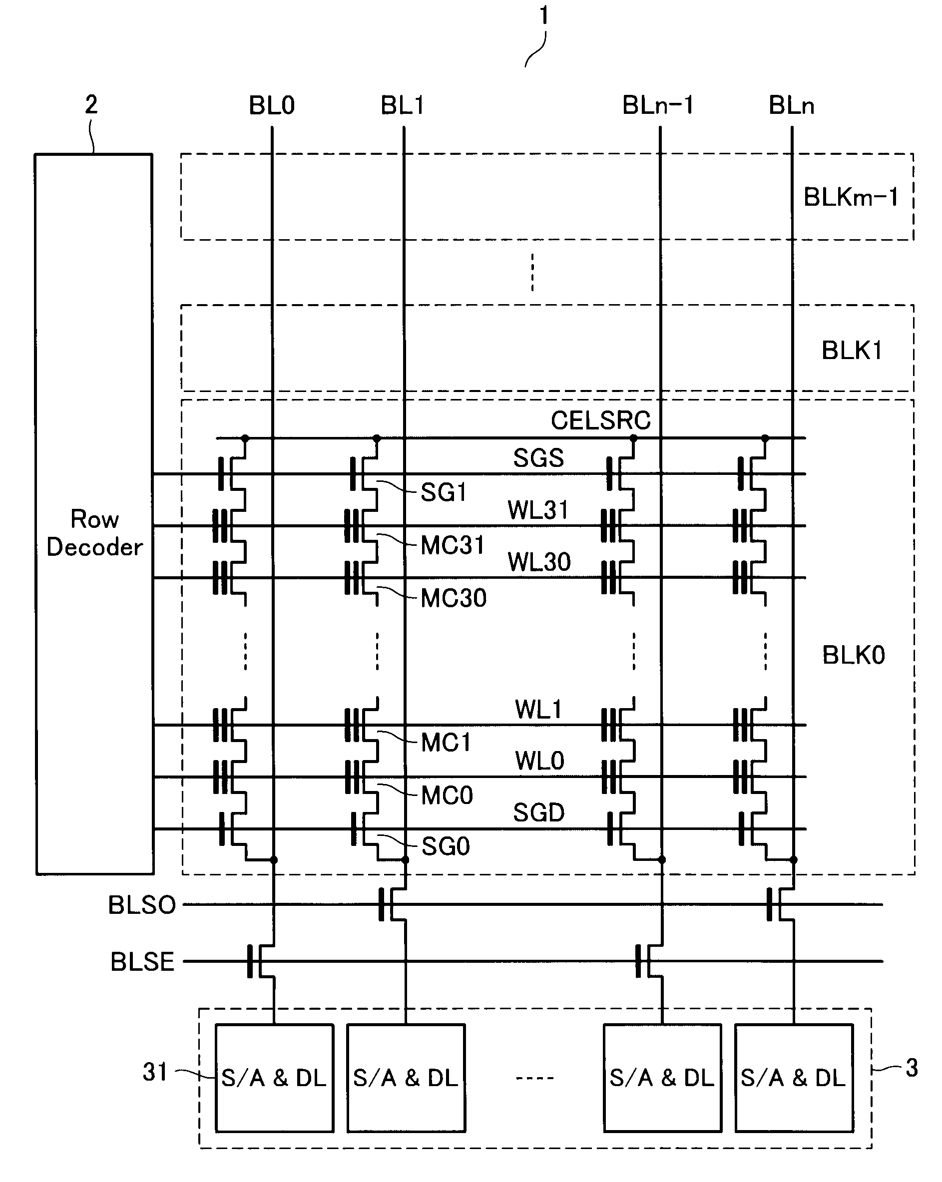
[0022]FIG. 1 shows a memory core configuration of a multi-value NAND type flash memory according to a first embodiment. A memory cell array 1 is configured as an array of NAND cell units (NAND strings) each including a plurality of electrically rewritable nonvolatile memory cells MC0 to MC31 connected in series.

[0023]One end of each NAND cell unit is connected to a bit line BL via a select gate transistor SG0, and the other end thereof is connected to a source line CELSRC via a select gate transistor SG1. The control gates of the memory cells MC0 to MC31 in the NAND cell unit are connected to different word lines WL0 to WL31. The gates of the select gate transistors SG0 and SG1 are connected to select gate lines SGD and SGS extending in parallel with the word lines WL.

[0024]There is provided a row decoder 2, which is a part of a writing circuit for selecting and driving the word lines WL and the select gate lines SGD and SGS. Each bit line BL is connected to a sense amplifier and da...

second embodiment

[0050]The second embodiment is another example of the first embodiment modified in the program operation, and identical with the first embodiment except the operation waveforms of the bit lines.

[0051]FIG. 5 shows operation waveform charts of a selected word line WL and bit lines BL according to the present embodiment. Since the operation of the selected word line WL is the same as the first embodiment shown in FIG. 4, explanation will not be given thereon.

[0052]First, a bit line BL(C) is lowered from a non-selected level to a selected level at the same timing as the start of the first section Ppc of a writing pulse (step S201). During the section Ppc, the bit lines BL(B) and BL(A) remain at a non-selected level.

[0053]Next, at the same timing as the end of the section Ppc (the start of the section Ppb), the bit line BL(C) is raised from the selected level by a voltage ΔVs (step S202), and the bit line BL(B) is lowered from a non-selected level to a selected level (step S203). During ...

third embodiment

[0059]The third embodiment is another example of the first embodiment modified in the program operation, and identical with the first embodiment except the step width of the writing pulse (step width is the width of increase in the pulse height).

[0060]FIG. 6 is a diagram showing writing pulses and verify pulses according to the present embodiment. Since verify pulses are the same as those of the first embodiment shown in FIG. 3, explanation will not be given thereon.

[0061]According to the present embodiment, the step widths between the writing pulse of a given writing cycle and the writing pulse of the next writing cycle are voltages ΔVpa, ΔVpb, and ΔVpc, which are varied among the different sections Ppa to Ppc.

[0062]In FIG. 6, the step widths ΔVpa to ΔVpc are in the relationship of “ΔVpc>ΔVpb>ΔVpa”. However, the step widths are not limited to this relationship, but optimum step widths may be set for the respective threshold levels.

[0063]In FIG. 6, the step widths between the writin...


PUM


Abstract

A nonvolatile semiconductor memory device according to an embodiment includes: a memory cell array including a plurality of memory cells to store N-value data (N being an integer equal to or larger than 3); and a writing circuit configured to repeatedly execute a writing cycle on a plurality of memory cells until data writing is finished. The writing circuit divides the pulse width of the writing pulse into a plurality of sections to change the pulse height among the sections such that the respective sections provide writing voltages for writing different target threshold levels, and brings the bit line connected to the memory cell to be written with any of the target threshold levels into a selected state synchronously to the section for applying the writing voltage for writing that target threshold level.

Description

CROSS REFERENCE TO RELATED APPLICATIONS[0001]This application is based on and claims the benefit of priority from prior Japanese Patent Application No. 2009-219089, filed on Sep. 24, 2009, the entire contents of which are incorporated herein by reference.BACKGROUND[0002]1. Field[0003]Embodiments described herein relate generally to a nonvolatile semiconductor memory device.[0004]2. Description of the Related Art[0005]One type of EEPROM is NAND type flash memory. Owing to its memory cell configuration having a small unit cell area of about 4F2 (F: minimum feature size), NAND type flash memory leads other nonvolatile semiconductor memories in suitability for miniaturization and large memory capacity. If multi-value storage technique of storing data of two bits or more in one memory cell is used, the memory capacity can be increased to double or higher without increase in the chip area.[0006]Nowadays, NAND type flash memory is used as nonvolatile recording media of various portable gad...

Claims


Application Information

Patent Timeline
IPC IPC(8): G11C16/04G11C16/12
CPCG11C11/5628G11C2211/5621G11C16/3454G11C16/0483
Inventor WATANABE, YOSHIHISA
Owner KK TOSHIBA
Why Eureka
Try Eureka