Electronic device

a technology of electronic devices and interconnects, applied in the field of electronic devices, can solve the problems of increasing device size, increasing line width, and prone to disconnection of interconnects, and achieve the effect of effectively preventing the disconnection of interconnects and increasing the size of electronic devices

Inactive Publication Date: 2011-03-31
RENESAS ELECTRONICS CORP
View PDF2 Cites 2 Cited by
  • Summary
  • Abstract
  • Description
  • Claims
  • Application Information

AI Technical Summary

Benefits of technology

[0019]Thus, the present invention enables effectively preventing the disconnection of the interconnect formed on the substrate, without incurring an increase in size of the electronic device including the electronic component mounted on the substrate.

Problems solved by technology

The conventional substrate with the electronic component mounted thereon, however, has a drawback that the interconnect is prone to suffer disconnection.
In order to increase the line width of the interconnect the pitch between the external terminals has to be extended, however this incurs a disadvantage that the device size has to be increased.
Such configuration inhibits increasing the line width of the interconnect in the inner region, and is hence unable to solve the foregoing problem of the disconnection.

Method used


Image

  • Electronic device
  • Electronic device
  • Electronic device

Examples


Embodiment Construction

[0032]The invention will be now described herein with reference to illustrative embodiments. Those skilled in the art will recognize that many alternative embodiments can be accomplished using the teachings of the present invention and that the invention is not limited to the embodiments illustrated for explanatory purposes.

[0033]Hereunder, an embodiment of the present invention will be described in details, referring to the drawings. In all the drawings, the same constituents will be given the same numeral, and the description thereof will not be repeated.

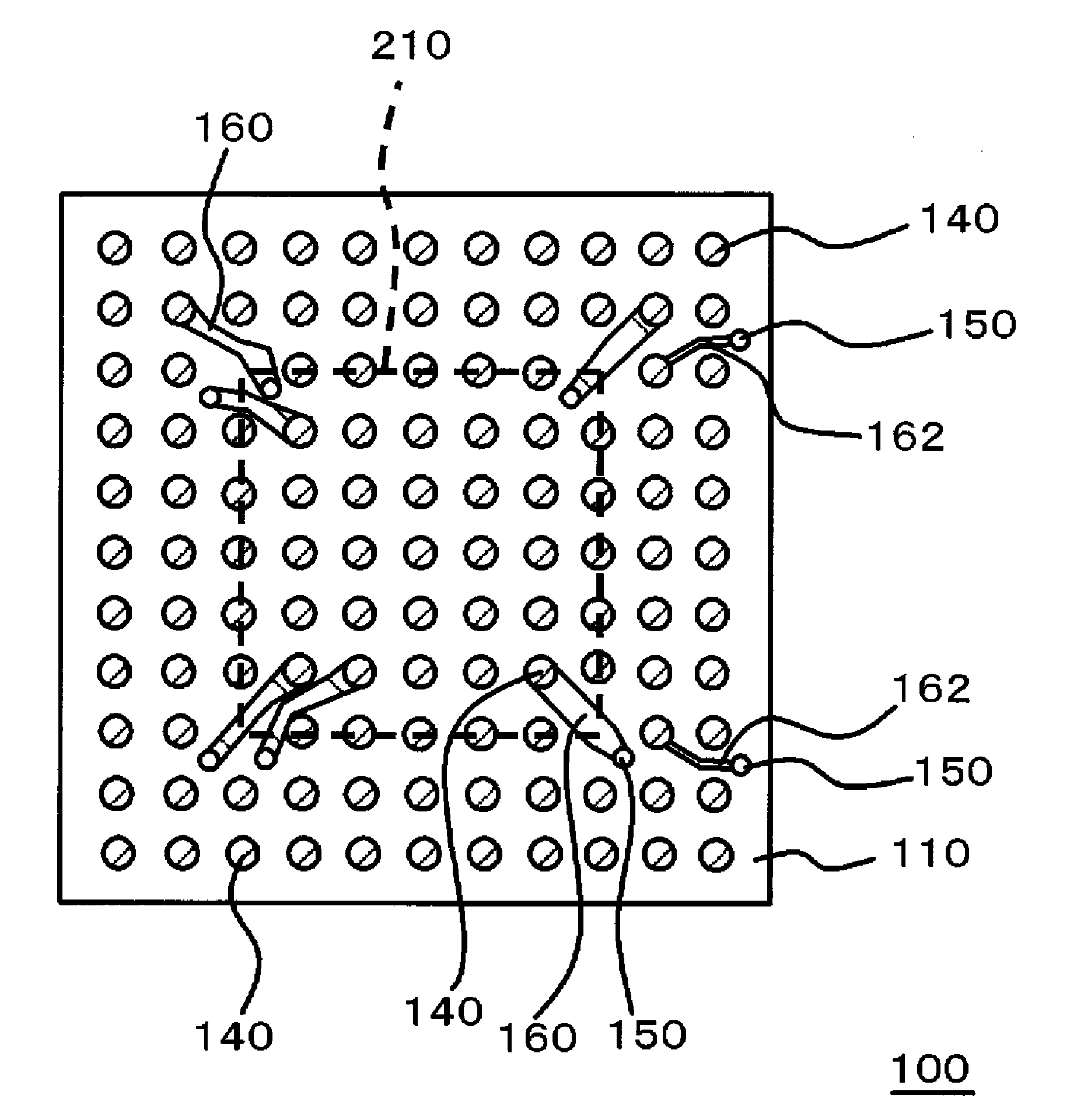
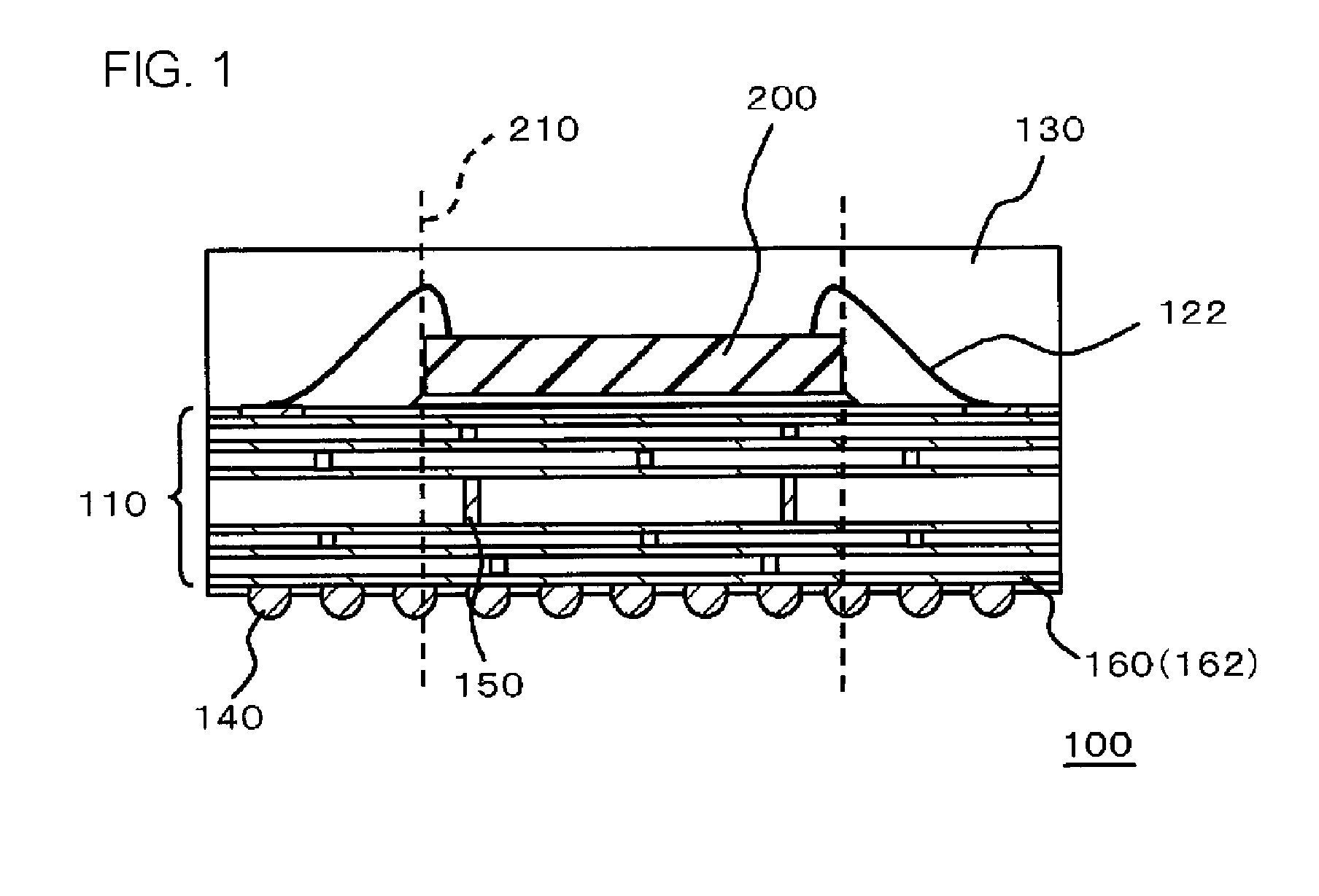
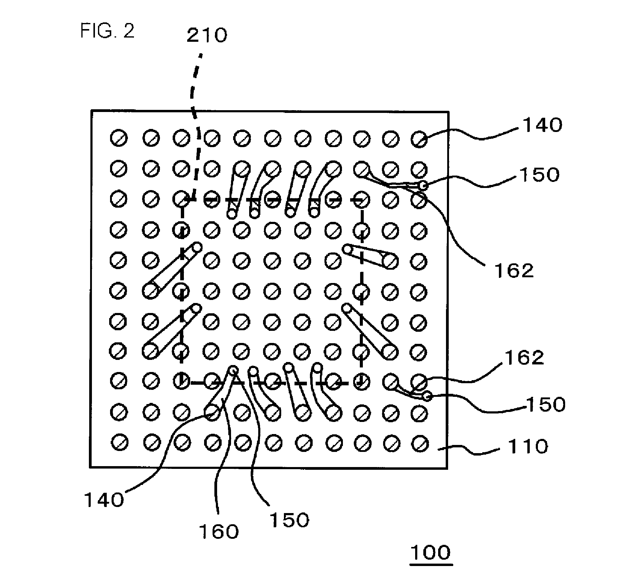
[0034]FIG. 1 is a cross-sectional view showing a structure of an electronic device according to this embodiment.

[0035]The electronic device 100 includes a substrate 110, an electronic component 200 mounted on a main surface (upper face according to the orientation of FIG. 1) of the substrate 110, and a plurality of external terminals 140 provided on a back surface (lower face according to the orientation of FIG. 1) of the substrat...


PUM


Abstract

The electronic device includes the substrate, the electronic component mounted on a main surface of the substrate, a plurality of external terminals formed on a back surface of the substrate, and a plurality of interconnects formed on the back surface of the substrate, wherein the plurality of interconnects includes a first interconnect disposed so as to overlap with an outer edge of the electronic component in a plan view. A pitch between a first external terminal and a second external terminal, adjacent to each other in one direction with the first interconnect located therebetween, is wider than a pitch between a third external terminal and a fourth external terminal, adjacent to each other in the same direction without the first interconnect located therebetween.

Description

[0001]This application is based on Japanese patent application No. 2009-221198, the content of which is incorporated hereinto by reference.BACKGROUND[0002]1. Technical Field[0003]The present invention relates to an electronic device, and more particularly to en electronic device including an electronic component mounted on a substrate.[0004]2. Related Art[0005]In the electronic device formed in a package structure, which includes an electronic component such as a semiconductor element mounted on a main surface of a substrate, a plurality of external terminals such as solder balls is provided on a back surface of the substrate opposite to the main surface, for connecting the electronic device to a terminal of an external substrate such as a mother board or a printed circuit board. On such back surface of the substrate, also, an interconnect is provided for electrically connecting the external terminal and a via formed in the substrate. The external terminal is electrically connected ...

Claims


Application Information

Patent Timeline
Patent Type & Authority Applications(United States)
IPC IPC(8): H01L23/48
CPCH01L23/49816H01L23/49838H01L24/48H01L2224/48091H01L2924/15311H01L2924/14H01L2924/00014H01L2224/73265H01L2924/181H01L2924/00012H01L2224/45099H01L2224/45015H01L2924/207
Inventor TSUKUDA, TATSUAKI
Owner RENESAS ELECTRONICS CORP
Why Eureka
Try Eureka