Electroluminescent device aging compensation with reference subpixels

a reference subpixel and electroluminescent device technology, applied in the direction of electric digital data processing, instruments, computing, etc., can solve the problems of reducing the lifetime of the device, differential color aging, and aging of the organic materials of the device, so as to accurately compensate for the aging of the organic materials, the effect of reducing efficiency loss and accurate compensation

Active Publication Date: 2011-03-31
GLOBAL OLED TECH
View PDF13 Cites 175 Cited by
  • Summary
  • Abstract
  • Description
  • Claims
  • Application Information

AI Technical Summary

Benefits of technology

[0018]An advantage of this invention is an OLED device that accurately compensates for the aging of the organic materials in the device for each subpixel, by measuring electrical characteristics of the primary and reference EL emitters, even in the presence of manufacturing variations. By incorporating a plurality of reference EL emitters throughout the OLED device, spatial variations of the organic materials may be characterized, enabling accurate compensation throughout the OLED device. This invention can compensate for chromaticity shifts as well as for efficiency loss. It does not require pre-production measurements, and does not reduce aperture ratio or lifetime.

Problems solved by technology

However, as the device is used, the organic materials in the device age and become less efficient at emitting light.
This reduces the lifetime of the device.
The differing organic materials can age at different rates, causing differential color aging and a device whose white point varies as the device is used.
In addition, each individual pixel can age at a rate different from other pixels, resulting in device nonuniformity.
However, many of these techniques require circuitry in the illumination area to measure the characteristics of each EL emitter.
Furthermore, these techniques require time-consuming measurements of representative devices before production to determine typical aging profiles.
Furthermore, this scheme measures voltage or capacitance, so it cannot directly sense a change in light output due to a change in EL emitter efficiency, or a change in chromaticity of the light emitted by the EL emitter.
However, this scheme does not compensate for nonuniformity due to differential aging of adjacent subpixels, and does not compensate for chromaticity shift.
However, since this scheme uses curves taken before manufacturing, it cannot compensate for variations in those curves between individual panels, or for long-term shifts in the average characteristics of the displays manufactured due to aging of equipment, process changes, or material changes.
However, this scheme can reduce aperture ratio and reduce lifetime as described above.

Method used


Image

  • Electroluminescent device aging compensation with reference subpixels
  • Electroluminescent device aging compensation with reference subpixels
  • Electroluminescent device aging compensation with reference subpixels

Examples


Embodiment Construction

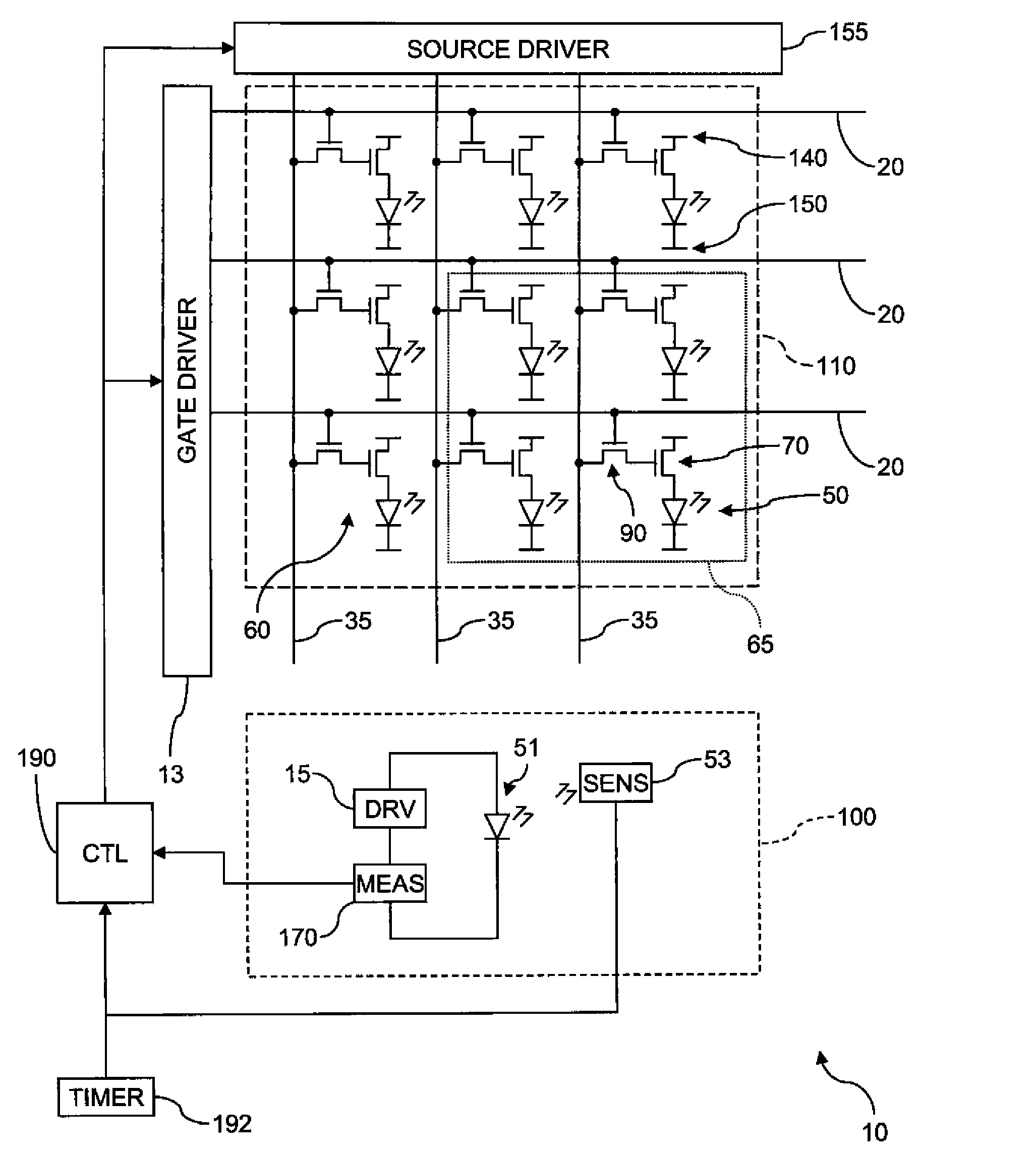
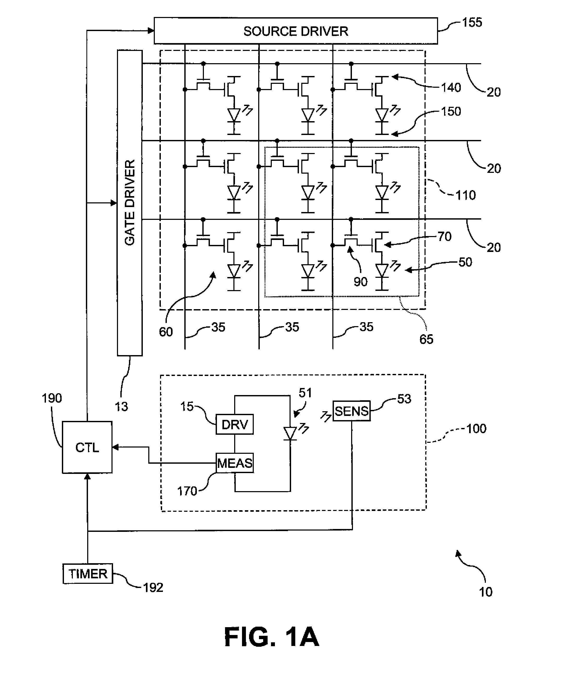
[0032]FIG. 1A shows an electroluminescent (EL) device 10 which can be used to compensate for aging of EL emitters 50. EL device 10 can be an active-matrix EL display or programmable active-matrix EL lamp or other light source. EL device 10 includes an illumination area 110 containing a matrix of primary subpixels 60 arranged in rows and columns, each primary subpixel 60 having a primary EL emitter 50, a drive transistor 70 and a select transistor 90, and being connected to first voltage source 140 and second voltage source 150. Each row of primary subpixels 60 is connected to a select line 20, and each column of primary subpixels 60 is connected to a data line 35. The select lines are controlled by gate driver 13, and the data lines are controlled by source driver 155. Pixel 65 includes multiple EL subpixels 60, such as a red, a green, and a blue subpixel, or a red, a green, a blue, and a white subpixel. Pixel 65 can be arranged in quad, stripe, delta or other pixel patterns known i...


PUM


Abstract

An electroluminescent (EL) device including an illumination area having one or more primary EL emitters; a reference area having a reference EL emitter; a reference driver circuit for causing the reference EL emitter to emit light while the EL device is active; a sensor for detecting light emitted by the reference EL emitter; and a measurement unit for detecting an aging-related electrical parameter of the reference EL emitter while it is emitting light. The device further includes a controller for receiving an input signal for each primary EL emitter in the illumination area, forming a corrected input signal from each input signal using the detected light and the aging-related electrical parameter, and applying the corrected input signals to the respective primary EL emitters in the illumination area.

Description

CROSS REFERENCE TO RELATED APPLICATIONS[0001]Reference is made to commonly-assigned, co-pending U.S. patent application Ser. No. 11 / 766,823, filed Jun. 22, 2007, entitled “OLED Display with Aging and Efficiency Compensations” by Levey et al (U.S. Patent Publication No. 2008 / 0315788), and to commonly-assigned, co-pending U.S. patent application Ser. No. 11 / 962,182, filed Dec. 21, 2007, entitled “Electroluminescent Display Compensated Analog Transistor Drive Signal” by Leon et al (U.S. Patent Publication No. 2009 / 0160740), the disclosures of which are incorporated by reference herein.FIELD OF THE INVENTION[0002]The present invention relates to solid-state electroluminescent (EL) devices, such as organic light-emitting diode (OLED) devices, and more particularly to such devices that compensate for aging of the electroluminescent device components.BACKGROUND OF THE INVENTION[0003]Electroluminescent (EL) devices have been known for some years and have been recently used in commercial dis...

Claims


Application Information

Patent Timeline
Patent Type & Authority Applications(United States)
IPC IPC(8): G09G5/00
CPCG09G3/30G09G3/3208G09G2300/0465G09G2320/0242G09G2360/145G09G2320/041G09G2320/043G09G2360/141G09G2320/029G09G3/3233G09G3/32G09G3/3225G09G2300/0413G09G2320/04G09G2320/048
Inventor LEON, FELIPE A.WHITE, CHRISTOPHER J.
Owner GLOBAL OLED TECH
Why Eureka
Try Eureka