Semiconductor laser

a semiconductor laser and laser technology, applied in semiconductor lasers, laser details, electrical equipment, etc., can solve the problems of increasing cost, accumulating strain, and affecting the reliability of the wiring layer, so as to suppress the rotation of the plane of polarization caused by the stress applied on the ridge, the effect of reducing the deterioration of reliability

Inactive Publication Date: 2011-03-31
SONY CORP
View PDF5 Cites 12 Cited by
  • Summary
  • Abstract
  • Description
  • Claims
  • Application Information

AI Technical Summary

Benefits of technology

[0012]In a semiconductor laser according to an embodiment of the present invention, a stress which is applied when a filling material such as the insulating material is provided in the gap between the wiring layer and the inner wall of the trench is prevented from being applied to the ridge, so that rotation of the plane of polarization caused by the stress applied on the ridge is suppressed. In the case of forming the wiring layer by deposition, in a manufacturing process, there is no possibility that the wiring layers are in contact with each other, and deterioration in reliability caused by ultrasound occurs. Therefore, the ridges are driven independently of one another and, without deteriorating reliability, rotation of the angle of polarization caused by the stress applied on the ridge is suppressed. Further, according to the embodiment of the invention, accumulation of strains in the Au layer when the Au layer repeats expansion and shrink under severe environment is suppressed. Thus, the possibility that the wiring layer is broken is reduced.
[0013]In a semiconductor laser according to an embodiment of the present invention, a stress which is applied when a filling material such as the insulating material is provided in the gap between the wiring layer and the inner wall of the trench is prevented from being applied to the ridge. Therefore, rotation of the plane of polarization caused by the stress applied on the ridge is suppressed. In the case of forming the wiring layer by deposition, in a manufacturing process, there is no possibility that the wiring layers are in contact with each other, and deterioration in reliability caused by ultrasound occurs. Therefore, the ridges are driven independently of one another and, without deteriorating reliability, rotation of the plane of polarization caused by the stress applied on the ridge is suppressed. Further, according to the embodiment of the invention, accumulation of strains in the wiring layer when the wiring layer repeats expansion and shrink under severe environment is suppressed. Thus, the possibility that the wiring layer is broken is reduced.

Problems solved by technology

However, in the case of burying an isolation trench with an insulation material, stress is applied on the ridge due to shrinkage and strain of the buried insulating material, and the plane of polarization of a laser beam emitted from the ridge tends to rotate.
In the case where a deep isolation trench is formed, a process of filling with the insulating material becomes complicated, and a problem of increase in cost occurs.
, strain is accumulated in the Au layer, and there is the possibility that the wiring layer is broken.

Method used


Image

  • Semiconductor laser
  • Semiconductor laser
  • Semiconductor laser

Examples


first embodiment

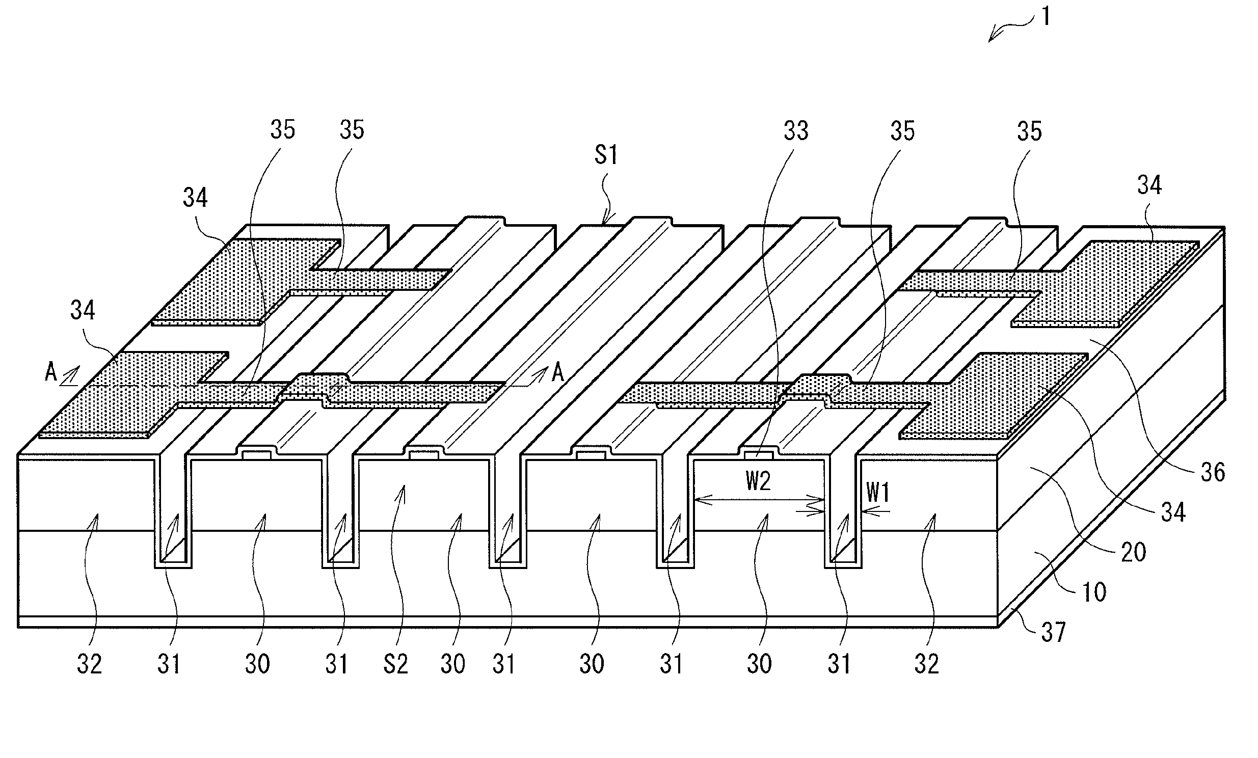
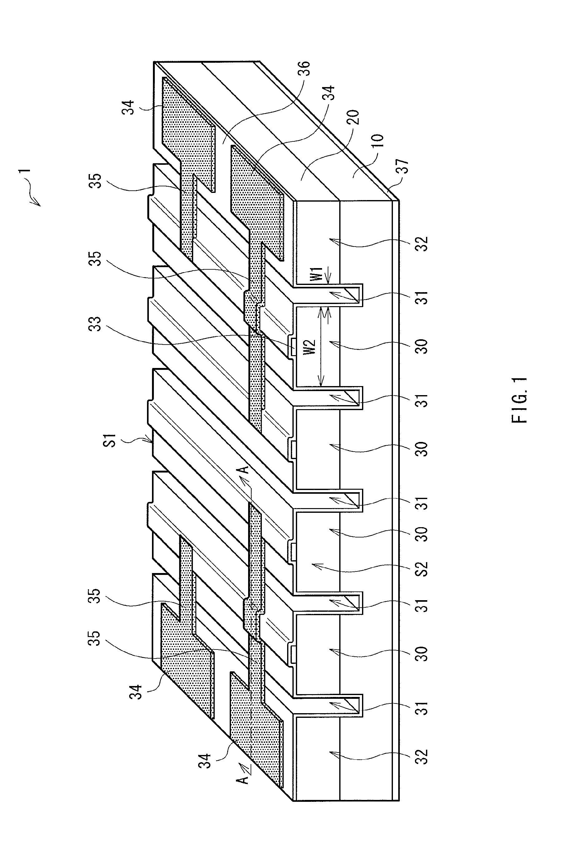
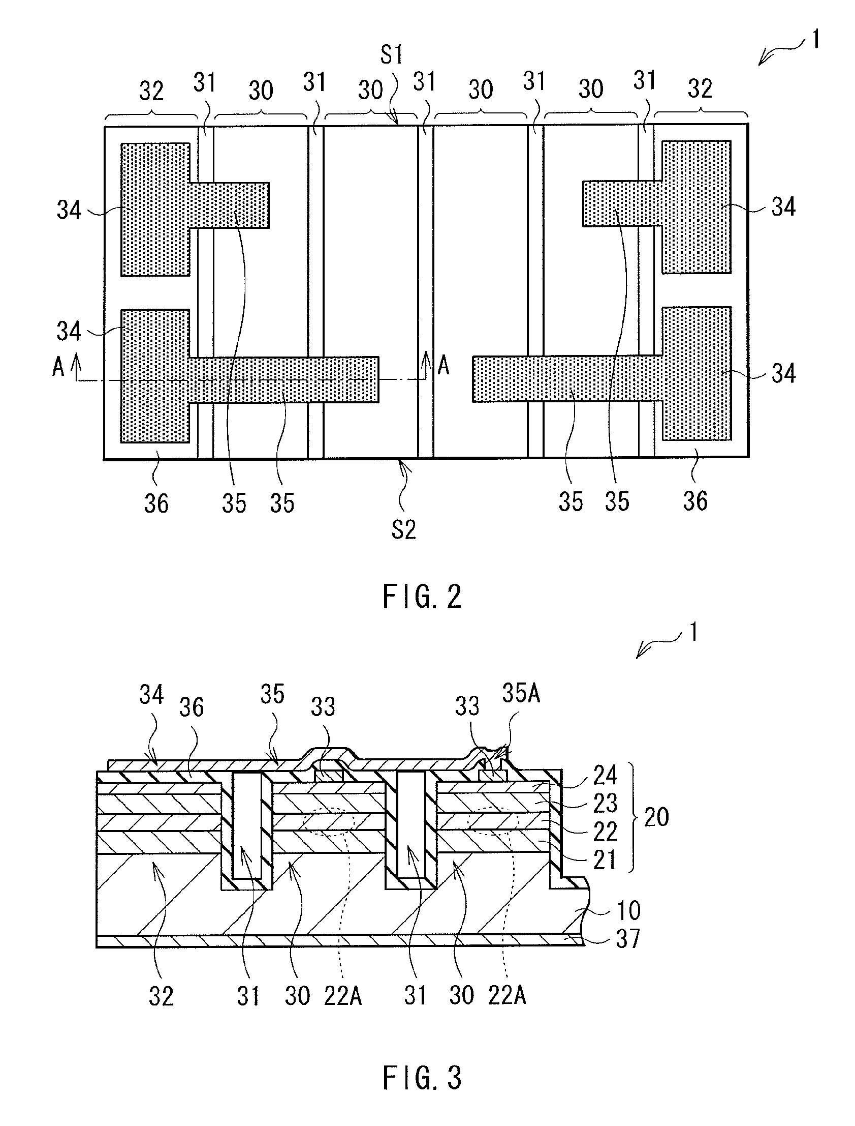
[0035]FIG. 1 is a perspective view illustrating an example of a schematic configuration of a semiconductor laser 1 according to a first embodiment of the present invention. FIG. 2 illustrates an example of the configuration of a top surface of the semiconductor laser 1 in FIG. 1. FIG. 3 illustrates an example of a sectional configuration taken along line A-A of the semiconductor laser 1 in FIG. 1 or 2. The semiconductor laser 1 of the embodiment is a multi-beam semiconductor laser having a plurality of stripe-shaped emitters and an edge-emitting semiconductor laser for emitting a laser beam from end surfaces of the emitters.

[0036]The semiconductor laser 1 has, for example, a semiconductor layer 20 on a substrate 10. The semiconductor layer 20 includes, for example, as illustrated in FIG. 3, a lower cladding layer 21, an active layer 22, an upper cladding layer 23, and a contact layer 24 in order from the substrate 10 side. Although not illustrated, the semiconductor layer 20 may be ...

second embodiment

Modification of Second Embodiment

[0069]In the second embodiment, a portion disposed in the air in the wiring layer 35 has an arch shape which projects toward the side opposite to the bottom surface of the trench 31. For example, although not illustrated, the portion may have a flat shape or a concave shape which dents toward the trench side. Also in the case where the wiring layer 35 has such a shape, accumulation of strains in the Au layer 35C is suppressed, and the possibility that the wiring layer 35 is broken is reduced.

example

[0070]Next, an example of the semiconductor lasers 1 and 2 according to the foregoing embodiments will be described in contrast with a comparative example. As an example of the semiconductor laser 1, the portion disposed in the air in the wiring layer 35 was formed in a flat shape, and a Ti layer, a Pt layer, and an Au layer were stacked in this order on the top surface side of the ridge 30. As an example of the semiconductor laser 2, the portion disposed in the air in the wiring layer 35 was formed in an arch shape which projects toward the side opposite to the bottom surface of the trench 31, and the adhesion layer 35B obtained by stacking a Ti layer and a Pt layer in this order from the trench 31 side, the Au layer 35C, and the strain suppression layer 35D made of Ti or Ni were stacked in this order from the trench 31 side. In a comparative example, the portion disposed in the air in the wiring layer 35 was formed in an arch shape which projects toward the side opposite to the bo...


PUM


Abstract

The present invention provides a semiconductor laser realizing reduced possibility that a wiring layer disposed in the air is broken even under severe environment of a large temperature difference. A trench is provided between adjacent ridges, and a wiring layer electrically connecting an upper electrode and a pad electrode is disposed in the air at least above the trench. The wiring layer in a portion above the trench has a flat shape or a concave shape which dents toward the trench. With the configuration, accumulation of strains in the wiring layer when the wiring layer repeats expansion and shrink under severe environment of a large temperature difference is suppressed.

Description

BACKGROUND OF THE INVENTION[0001]1. Field of the Invention[0002]The present invention relates to a semiconductor laser in which emitters are driven independently of one another.[0003]2. Description of the Related Art[0004]In a semiconductor laser, to drive emitters independently of one another, an isolation trench for electrically isolating adjacent emitters is provided between the adjacent emitters. The width of the isolation trench is, though it varies depending on the types of lasers, only a few μm in the case of a laser of a narrow-pitch type in which a beam pitch is tens μm. Consequently, in such a case, it is extremely difficult to provide a wiring layer that couples a stripe electrode on an emitter (ridge) sandwiched by isolation trenches and a pad electrode formed in a place apart from the ridge in the narrow isolation trench. Therefore, for example, as described in Japanese Unexamined Patent Application Publication No. 2000-269601, generally, an insulating material is burie...

Claims


Application Information

Patent Timeline
Patent Type & Authority Applications(United States)
IPC IPC(8): H01S5/02
CPCH01S5/0425H01S5/22H01S5/02276H01S2301/176H01S5/4031H01S5/04252H01S5/04256H01S5/02345
Inventor KURAMOCHI, HISAYOSHIHINO, TOMONORIHIRATA, TATSUHIROYOSHIDA, YUTA
Owner SONY CORP
Why Eureka
Try Eureka