Manufacturing method of semiconductor device

a manufacturing method and semiconductor technology, applied in the direction of semiconductor devices, semiconductor/solid-state device details, electrical equipment, etc., can solve the problems of deterioration in and achieve the effect of improving the reliability of manufactured semiconductor devices

Inactive Publication Date: 2011-03-31
RENESAS ELECTRONICS CORP
View PDF4 Cites 14 Cited by
  • Summary
  • Abstract
  • Description
  • Claims
  • Application Information

AI Technical Summary

Benefits of technology

[0008]However, as the semiconductor device becomes higher in functionality and integration, the number of the electrode pads of the electronic components (including a semiconductor chip and the chip components) mounted on the second substrate or the number of the electronic components mounted on the second substrate tends to increase. Accordingly, the number of the electrodes for electrically coupling the second substrate to the first substrate also tends to increase. As a result, electrodes disposed between the individual substrates act as an impediment and narrow a supply path for the sealing resin so that air tends to be easily contained in the supplied sealing resin, and may remain in a sealed body formed by the sealing step. If air remains in the sealed body, the reliability of the manufactured semiconductor device may deteriorate.
[0009]The present invention has been achieved in view of the foregoing problem, and an object of the present invention is to provide a technology which can improve the reliability of a semiconductor device.
[0010]Another object of the present invention is to provide a technology which allows miniaturization or higher integration of a semiconductor device.
[0015]That is, the reliability of a semiconductor device can be improved.

Problems solved by technology

If air remains in the sealed body, the reliability of the manufactured semiconductor device may deteriorate.

Method used


Image

  • Manufacturing method of semiconductor device
  • Manufacturing method of semiconductor device
  • Manufacturing method of semiconductor device

Examples


embodiment 1

General Description of Semiconductor Device

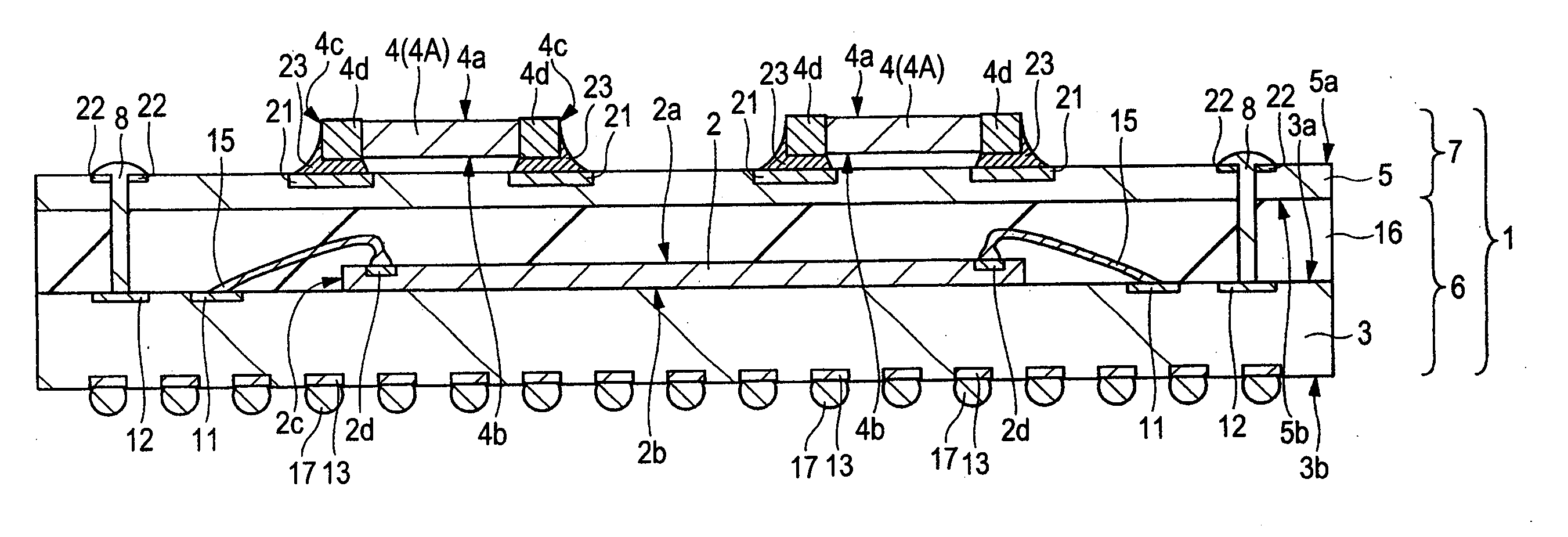
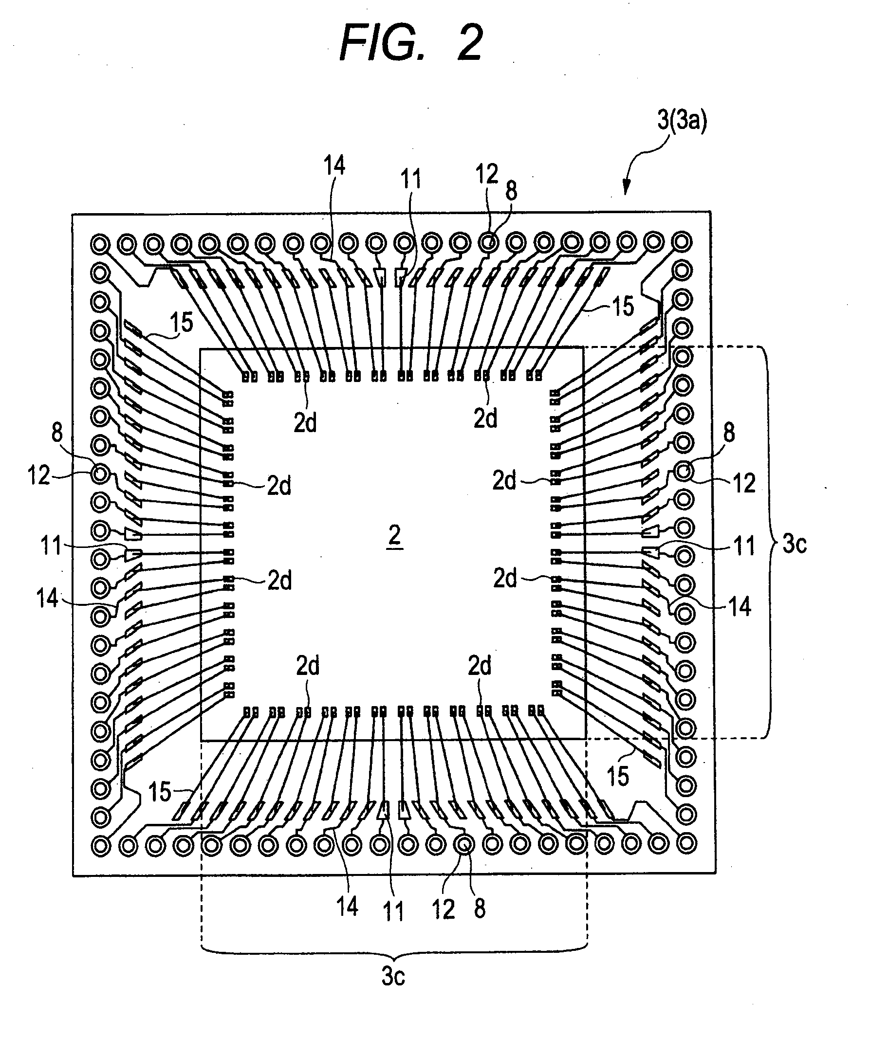
[0059]In the present embodiment, a Package-On-Package (POP) semiconductor device (hereinafter simply referred to as a POP) in which, over a wiring substrate (base member) having a semiconductor chip mounted thereon, another wiring substrate (base member) having an electronic component mounted thereon is stacked will be described as an example of a semiconductor device in which a plurality of wiring substrates each having an electronic component mounted thereon are stacked.

[0060]The POP includes, e.g., a lower-level wiring substrate having an electronic component such as a semiconductor chip mounted thereon, and an upper-level wiring substrate having an electronic component such as another semiconductor chip mounted thereon. By electrically coupling the upper-level wiring substrate to the lower-level wiring substrate via a conductive member, the upper-level electronic component is electrically coupled to the lower-level electronic component ...

embodiment 2

[0165]In the first embodiment described above, the description has been given to the implementation of the semiconductor device in which the two wiring substrates (base members) are stacked. However, the number of the wiring substrates to be stacked is not limited to two. In the second embodiment, a description will be given to an implementation in which three or more wiring substrates (base members) are stacked. Note that, in the present embodiment, the difference between the present embodiment and the first embodiment will be primarily described, and a description overlapping that in the first embodiment is omitted in principle.

[0166]FIG. 29 is a cross-sectional view showing an overall structure of a semiconductor device according to the present embodiment. The POP 60 according to the second embodiment shown in FIG. 29 is different from the POP 1 described above in the first embodiment in that the main surface 5a of a sub-substrate 63 mounted over the base substrate 3 is sealed wi...


PUM


Abstract

The reliability of a semiconductor device is improved. A sealing resin (sealed body) is formed between a sub-substrate (first base member) and a base substrate (second base member) that are provided individually and distinctly to be integrated therewith, and then, the sub-substrate is electrically coupled to the second base member. As a means for electrically coupling the sub-substrate to the base substrate, lands (first lands) formed on the sub-substrate and lands (second lands) formed on the base substrate are disposed such that the respective positions thereof are aligned. After through holes are formed from the lands of the sub-substrate toward the lands of the base substrate, a solder member (conductive member) is formed in each of the through holes.

Description

CROSS-REFERENCE TO RELATED APPLICATIONS[0001]The disclosure of Japanese Patent Application No. 2009-226679 filed on Sep. 30, 2009 including the specification, drawings and abstract is incorporated herein by reference in its entirety.BACKGROUND OF THE INVENTION[0002]The present invention relates to a technology for manufacturing an electronic device such as a semiconductor device, and particularly to a technology which is effective when applied to an electronic device (semiconductor device) in which, over the main surface of a base member having an electronic component such as a semiconductor chip mounted thereon, another wiring substrate is further stacked.[0003]In recent years, demand for the miniaturization of an electronic device such as a semiconductor device has increasingly grown stronger. Accordingly, it is assumed that forming each of a plurality of electronic components from one semiconductor device is effective in reducing a mounting region for a semiconductor device, chip...

Claims


Application Information

Patent Timeline
Patent Type & Authority Applications(United States)
IPC IPC(8): H01L21/60
CPCH01L21/561H01L21/565H01L23/3128H01L23/49816H01L23/49833H01L24/45H01L24/48H01L24/97H01L25/16H01L25/50H01L2224/45144H01L2224/48091H01L2224/48227H01L2224/48465H01L2224/49171H01L2224/97H01L2924/01004H01L2924/01014H01L2924/01029H01L2924/01047H01L2924/0105H01L2924/01075H01L2924/01078H01L2924/01079H01L2924/01082H01L2924/14H01L2924/15173H01L2924/15311H01L2924/15331H01L2924/19041H01L2924/01005H01L2924/01006H01L2924/01033H01L2924/014H01L24/49H01L2224/32225H01L2224/73265H01L2924/3511H01L25/0652H01L2924/01028H01L2924/00014H01L2224/85H01L2924/00H01L2924/00012H01L24/73H01L2224/05553H01L2924/15787H01L2924/181
Inventor HIRAI, TATSUYAHASHIMOTO, TOMOAKIKIKUCHI, TAKASHIYASUNAGA, MASATOSHISUGIYAMA, MICHIAKI
Owner RENESAS ELECTRONICS CORP
Why Eureka
Try Eureka