Multilayer substrate

a multi-layer substrate and substrate technology, applied in the direction of printed circuit aspects, printed circuit manufacturing, high-frequency circuit adaptations, etc., can solve the problems of strip not being able to connect to ground vias, difficult to use such approaches in high-density configurations, and inability to apply shielding structure between signal vias, etc., to achieve the effect of improving impedance matching and reducing crosstalk effects

Active Publication Date: 2011-04-07
NEC CORP
View PDF7 Cites 9 Cited by
  • Summary
  • Abstract
  • Description
  • Claims
  • Application Information

AI Technical Summary

Benefits of technology

[0008]It is an objective of the present invention to provide a multilayer substrate providing high-density vertical interconnections with improved impedance matching and reduced crosstalk effects between vertical interconnections.

Problems solved by technology

Therefore, improvement of impedance control and increase of density in the vertical interconnections satisfying simultaneously crosstalk requirements are complicated issues on a way in promotion higher speed in the systems.
However, in high-density configurations, such shielding structure can not be applied between signal vias due to dimensional tolerances of a via fabrications process.
At these layers, the strip cannot be connected to the ground vias due to the difference in the potential.
In this case, however, it is also difficult to use such approach in high-density configurations.

Method used


Image

  • Multilayer substrate
  • Multilayer substrate
  • Multilayer substrate

Examples


Embodiment Construction

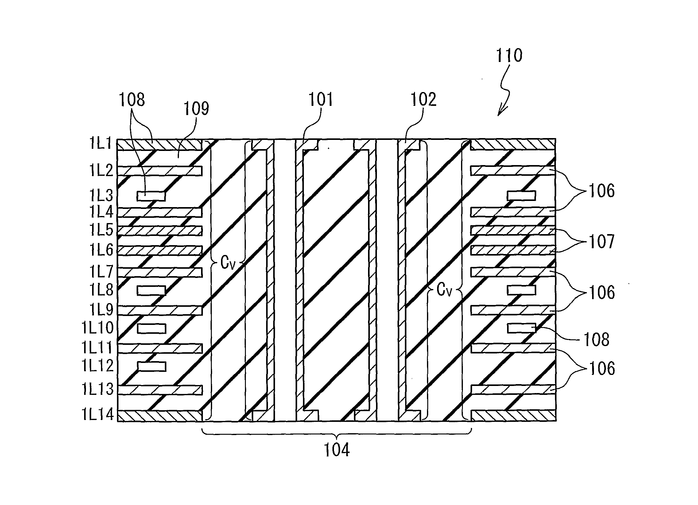
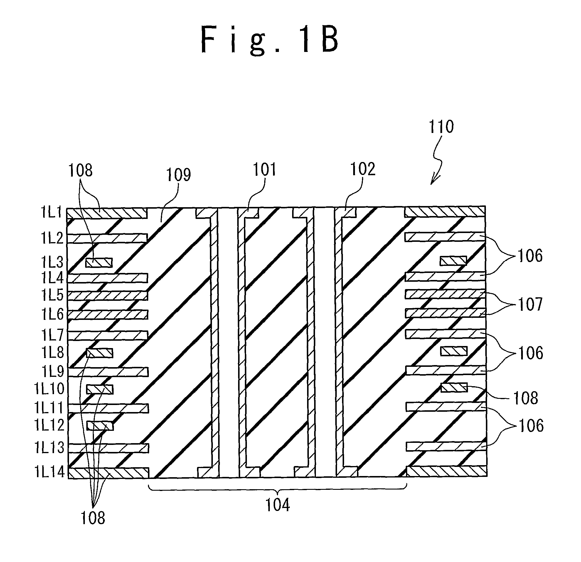
[0031]Hereinafter, several types of multilayer substrates comprising via structures in which conductive posts are used between signal vias to reduce coupling and finally crosstalk effects in whole high-speed interconnected structures formed in the multilayer substrates.

[0032]In an exemplary embodiment, as shown in FIGS. 1A to 1D, a multilayer substrate 110 is provided with a plurality of conductor layers, denoted by the numerals 1L1 to 1L14. Provided at the respective conductor layers 1L1 to 1L14 are conductor planes isolated by dielectric material 109. These conductor planes include ground planes 106, power supply planes 107, and signal layers 108.

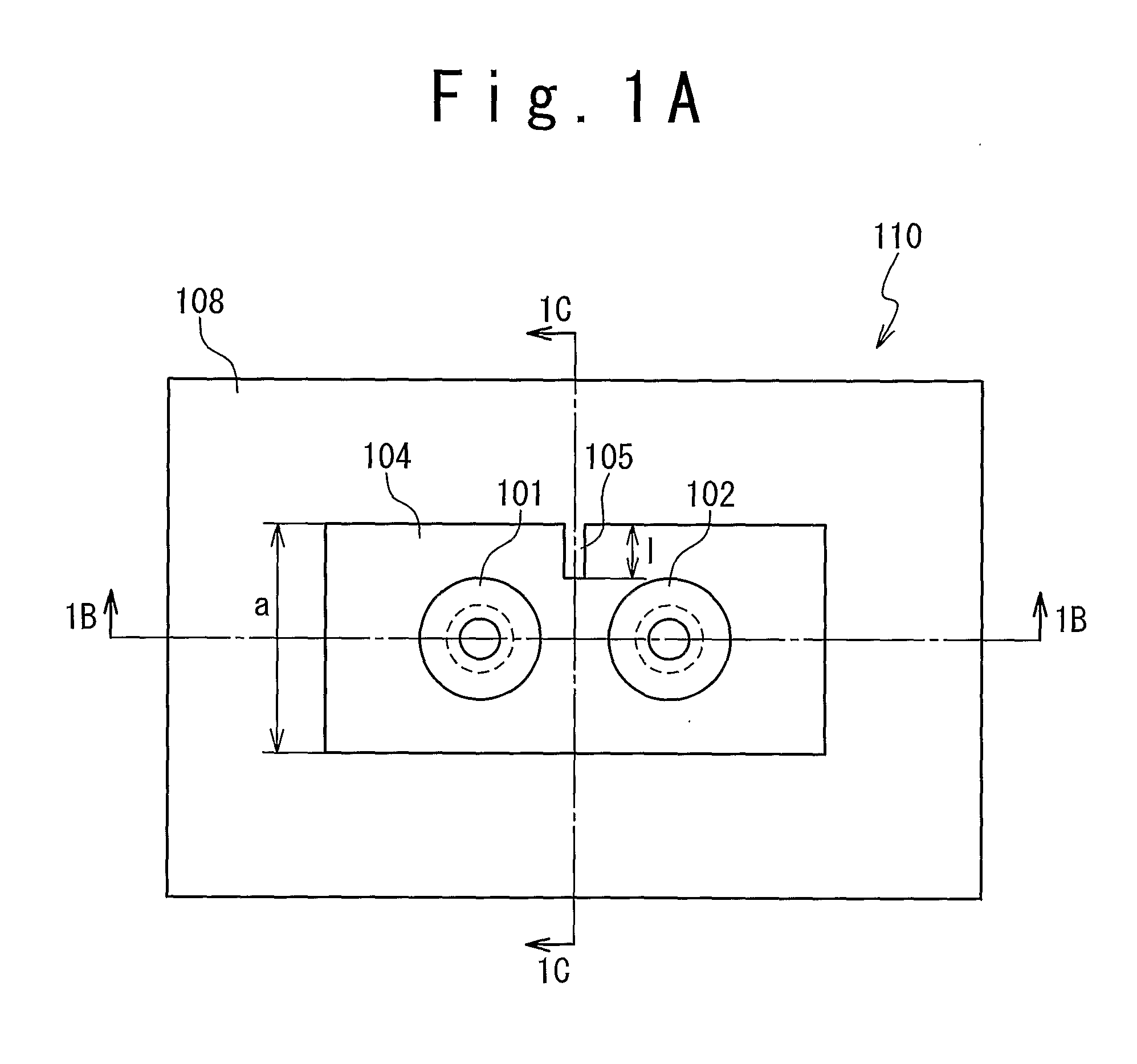
[0033]The multilayer substrate 110 is composed of a conductor plane region and a clearance region. The conductor planes are provided only in the conductor plane region; the conductor planes are excluded from the clearance region 104. In FIGS. 1A-1D, the clearance region is denoted by the numeral 104.

[0034]Signal vias 101 and 102 are dispo...


PUM


Abstract

A multilayer substrate is provided with a conductor plane region in which a plurality of conductor planes are disposed; a clearance region disposed adjacent to the conductor plane region so that the plurality of conductor planes are excluded from the clearance region. A plurality of signal vias are disposed through the clearance region so that the plurality of signal vias are isolated from the plurality of conductor planes. A conductor post is connected to one of the plurality of conductor planes and disposed between two of the signal vias in the clearance region.

Description

TECHNICAL FIELD[0001]The present invention relates to a multilayer substrate, including a multilayer printed circuit board, with reduced crosstalk between vertical transitions disposed in the substrate.BACKGROUND ART[0002]Both high-speed and high-density data transmission channels are a request of modern and next-generation supercomputing and networking systems. Implementation of electrical wiring technologies for such channels requires overcoming a number of difficulties such as impedance matching problems, crosstalk effects, unwanted resonances, and so on.[0003]Vertical interconnections connecting planar transmission lines disposed at different conductor layers are important elements to develop multilayer substrate technologies which are a cost-effective approach to dispose electrical wiring of high-speed systems. Therefore, improvement of impedance control and increase of density in the vertical interconnections satisfying simultaneously crosstalk requirements are complicated iss...

Claims


Application Information

Patent Timeline
Patent Type & Authority Applications(United States)
IPC IPC(8): H05K1/11
CPCH05K1/0245H05K1/0251H05K1/116H05K2201/09718H05K2201/09309H05K2201/09636H05K3/429
Inventor KUSHITA, TARASSAKAI, JUNKOUTA, HIKARU
Owner NEC CORP
Why Eureka
Try Eureka