Semiconductor memory device having diode cell structure

Inactive Publication Date: 2011-04-07
LONGITUDE LICENSING LTD
View PDF4 Cites 1 Cited by
  • Summary
  • Abstract
  • Description
  • Claims
  • Application Information

AI Technical Summary

Benefits of technology

[0008]The present invention seeks to solve one or more of the above problems and provides a semiconductor memory device capable of suppressing influence of temperature fluctuation of a diode and obtaining excellent sensing margin in a read operation of a memory cell including a phase change element and the diode.
[0010]According to the semiconductor memory device of the invention, in the read operation of the memory cell having a diode cell structure, a current flows from the first line applied with the first voltage to the second line applied with the second voltage through the memory cell, and the resistance state of the memory element is detected in accordance with a change in the current. At this point, since the first voltage has no temperature dependence and the second voltage has a temperature dependence opposite to that of the diode, it is possible to determine the resistance state of the memory element in a state where the temperature dependence of the forward voltage of the diode is cancelled. Thus, in the semiconductor memory device, excellent sensing margin can be obtained within a wide temperature range and the configuration of the control circuit can be simplified.
[0012]According to the present invention, in the semiconductor memory device employing the diode cell structure in which the memory cell is formed using the memory element and the diode, when the forward voltage of the diode has the temperature dependence, influence due to temperature fluctuation in reading the memory cell can be suppressed by giving an opposite temperature dependence to the second voltage. In this case, if the second voltage is set to a negative voltage, the first voltage can be set to a low positive voltage (for example, 0.5V). Therefore, it is possible to easily configure the control circuit (particularly, the read circuit) without using a boost voltage used in the conventional configuration.

Problems solved by technology

When forming a memory cell of the phase change memory device by using a MOS transistor, it is difficult to shrink the cell size in order to obtain a large gate width capable of flowing a large write current.
However, since current-voltage characteristics of the diode actually has a temperature dependence, the forward voltage of the diode fluctuates at low and high temperatures, which causes a risk that determination accuracy of the resistance state of the phase change element deteriorates.
However, in the configuration example of the Patent Reference 1, the boost voltage VSA applied to the bit line is drastically decreased when assuming the supply voltage of about 1 to 1.5V, and therefore voltage margin (sensing margin) of the read operation of the memory cell cannot be obtained.
That is, if the bit line voltage is decreased in a state where the word line is maintained at the ground potential, the voltage applied to the phase change element becomes small, and it becomes difficult to configure the read circuit for detecting the current change.
In this manner, in the conventional phase change memory device having the diode cell structure, there is a problem that the temperature fluctuation cannot be suppressed by cancelling the temperature dependence of the diode while obtaining the margin of the read operation.

Method used


Image

  • Semiconductor memory device having diode cell structure
  • Semiconductor memory device having diode cell structure
  • Semiconductor memory device having diode cell structure

Examples


Embodiment Construction

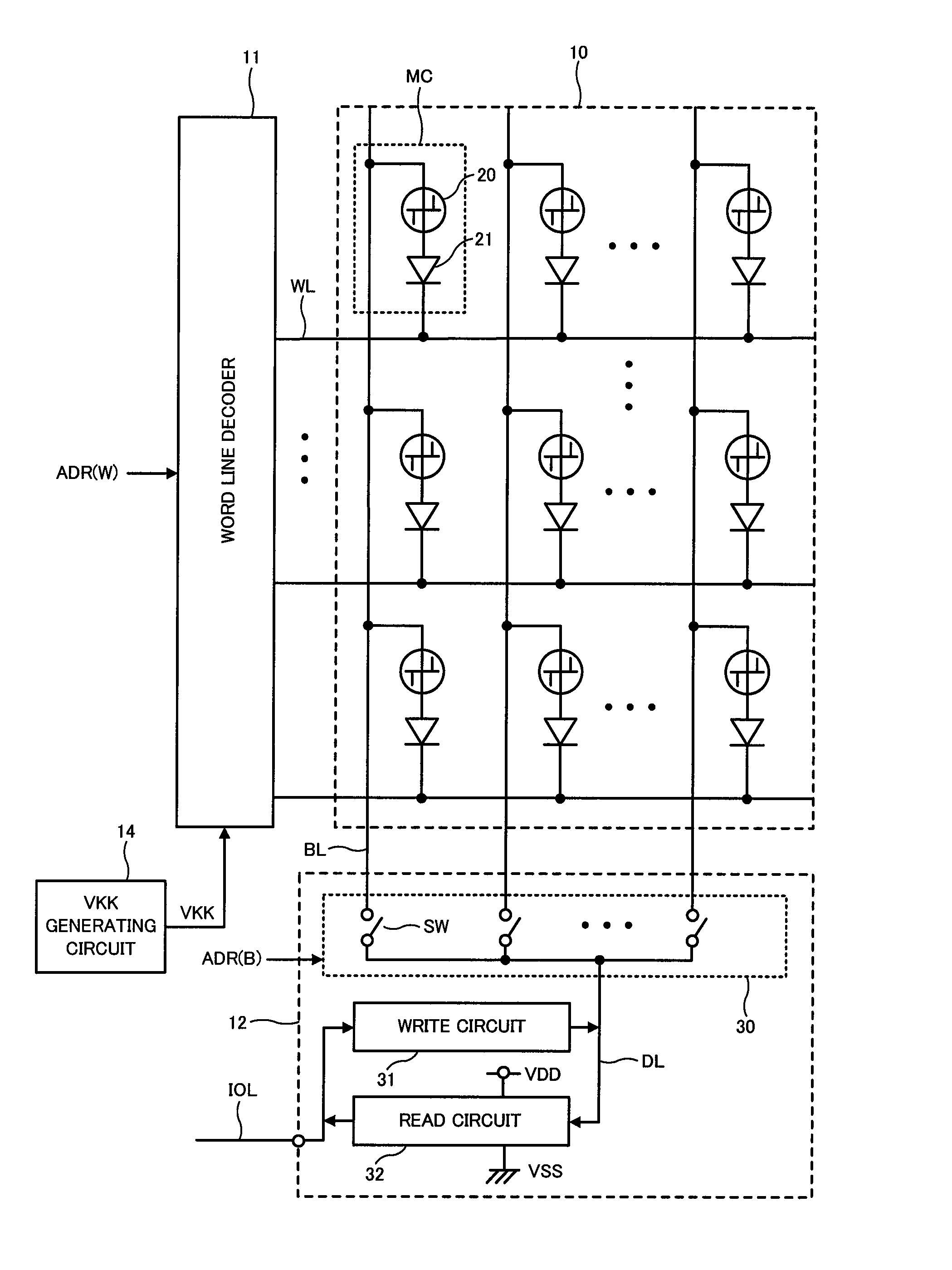
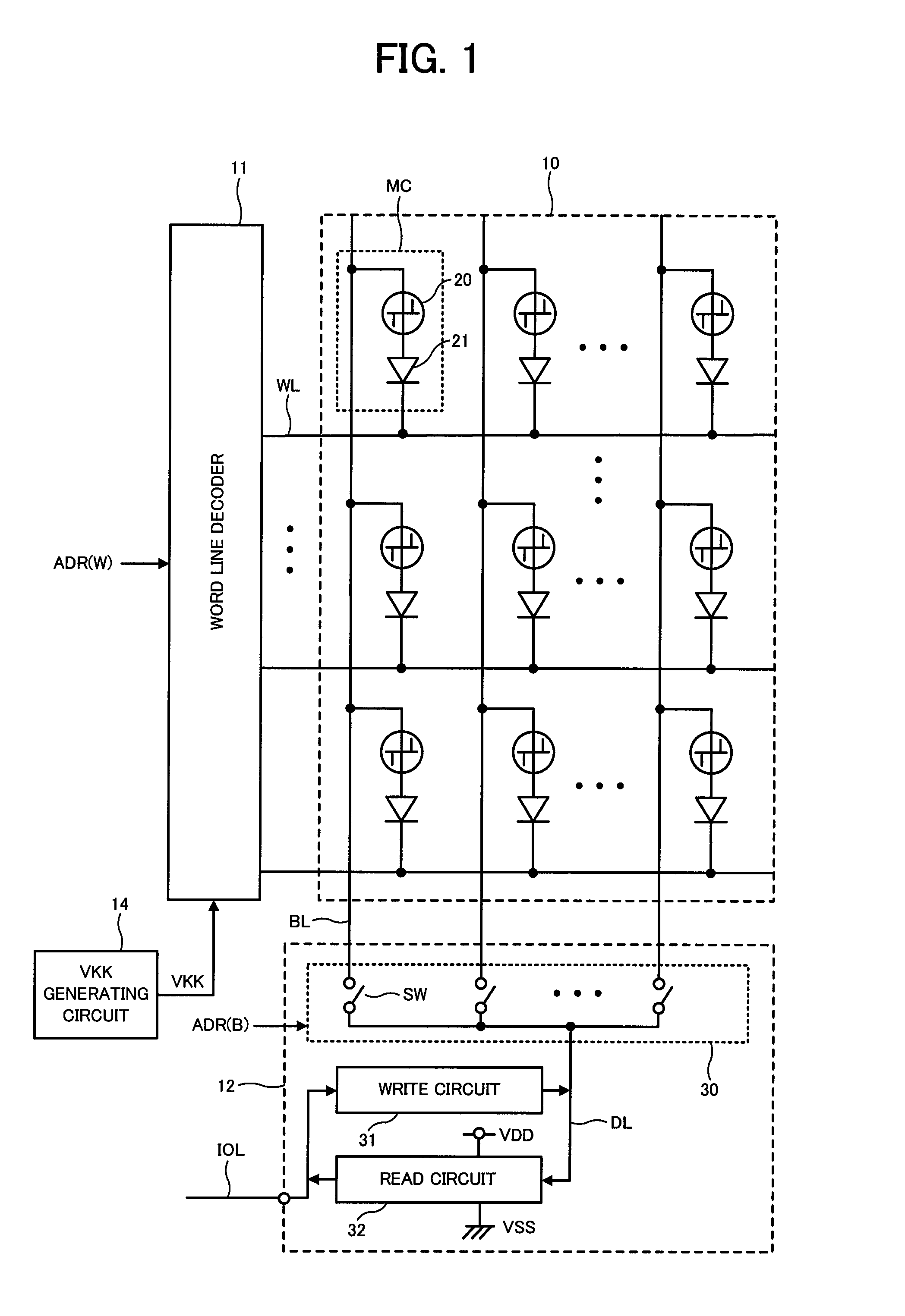
[0023]The invention will be now described herein with reference to illustrative embodiments. Those skilled in the art will recognize that many alternative embodiments can be accomplished using the teachings of the present invention and that the invention is not limited to the embodiments illustrated for explanatory purposes. In the following, the embodiments will be described in which the present invention is applied to a phase change memory device storing data in a memory cell employing the diode cell structure.

[0024]FIG. 1 is a diagram showing a basic configuration of the phase change memory device to which the present invention is applied. In FIG. 1, a memory cell array 10 includes a large number of memory cells MC arranged in a matrix, and there are provided a word line decoder 11, a bit line control circuit 12 and a VKK generating circuit 14 around the memory cell array 10. Further, the bit line control circuit 12 includes a bit line decoder 30, a write circuit 31 and a read ci...


PUM


Abstract

A semiconductor memory device comprises a memory cell, first and second voltage generating circuits generating first and second voltages, and a control circuit. A memory element and a diode included in the memory cell are connected in series between first and second lines. The first voltage has no temperature dependence, and the second voltage has a temperature dependence opposite to that of a forward voltage of the diode. The control circuit detects a resistance state of the memory element in accordance with a change in current flowing in the memory cell in a state where the first / second voltage is applied to the first / second in a read operation of the memory cell.

Description

BACKGROUND OF THE INVENTION[0001]1. Field of the Invention[0002]The present invention relates to a non-volatile semiconductor memory device for storing data using a change in resistance state of a memory element, and particularly relates to a semiconductor memory device in which a memory cell is formed by connecting the memory element and a diode in series.[0003]2. Description of Related Art[0004]A phase change memory device using structural change of phase change material is known as one of non-volatile semiconductor memory devices. The phase change memory device has a structure in which a resistance value of a phase change element made of the phase change material is changed by heat and thereby data can be rewritably stored. This heat is generated by flowing a large current in the phase change element. When forming a memory cell of the phase change memory device by using a MOS transistor, it is difficult to shrink the cell size in order to obtain a large gate width capable of flow...

Claims


Application Information

Patent Timeline
IPC IPC(8): G11C11/00
CPCG11C5/14G11C13/0004G11C2213/72G11C2213/15G11C13/004
Inventor TSUKADA, SHUICHI
Owner LONGITUDE LICENSING LTD
Why Eureka
Try Eureka