Cross point memory array devices

a technology of memory arrays and array devices, applied in semiconductor devices, digital storage, instruments, etc., can solve the problems of slow mim tunneling junction, unreliable, and lack of unidirectional switching functions,

Inactive Publication Date: 2011-04-14
NAN YA TECH
View PDF5 Cites 28 Cited by
  • Summary
  • Abstract
  • Description
  • Claims
  • Application Information

AI Technical Summary

Problems solved by technology

The layout of such devices is not ideal, usually requiring feature sizes of 8f2 for each memory cell, where f is the minimum feature size.
However, the MIM tunneling junction is slow, unreliable, and lacks unidirectional switching functions.
However, incorporating the p-n junction diode in a cross point memory is complex and it is difficult to scale down the p-n junction diode due to current supply limitations.
Crosstalk between adjacent memory cells, however, is the most critical issue for conventional cross point memory arrays, because the threshold voltage thereof is too small to resist noise.
The additional circuit and high-open-circuit voltage gain amplifier, however, occupies additional device space and increases fabrication complexity.

Method used


Image

  • Cross point memory array devices
  • Cross point memory array devices
  • Cross point memory array devices

Examples


Embodiment Construction

[0017]It is to be understood that the following disclosure provides many different embodiments, or examples, for implementing different features of various embodiments. Specific examples of components and arrangements are described below to simplify the present disclosure. These are merely examples and are not intended to be limiting. In addition, the present disclosure may repeat reference numerals and / or letters in the various examples. This repetition is for the purpose of simplicity and clarity and does not in itself indicate a relationship between the various embodiments and / or configurations discussed. Moreover, the formation of a first feature over or on a second feature in the description that follows may include embodiments in which the first and second features are formed in direct contact or not in direct contact.

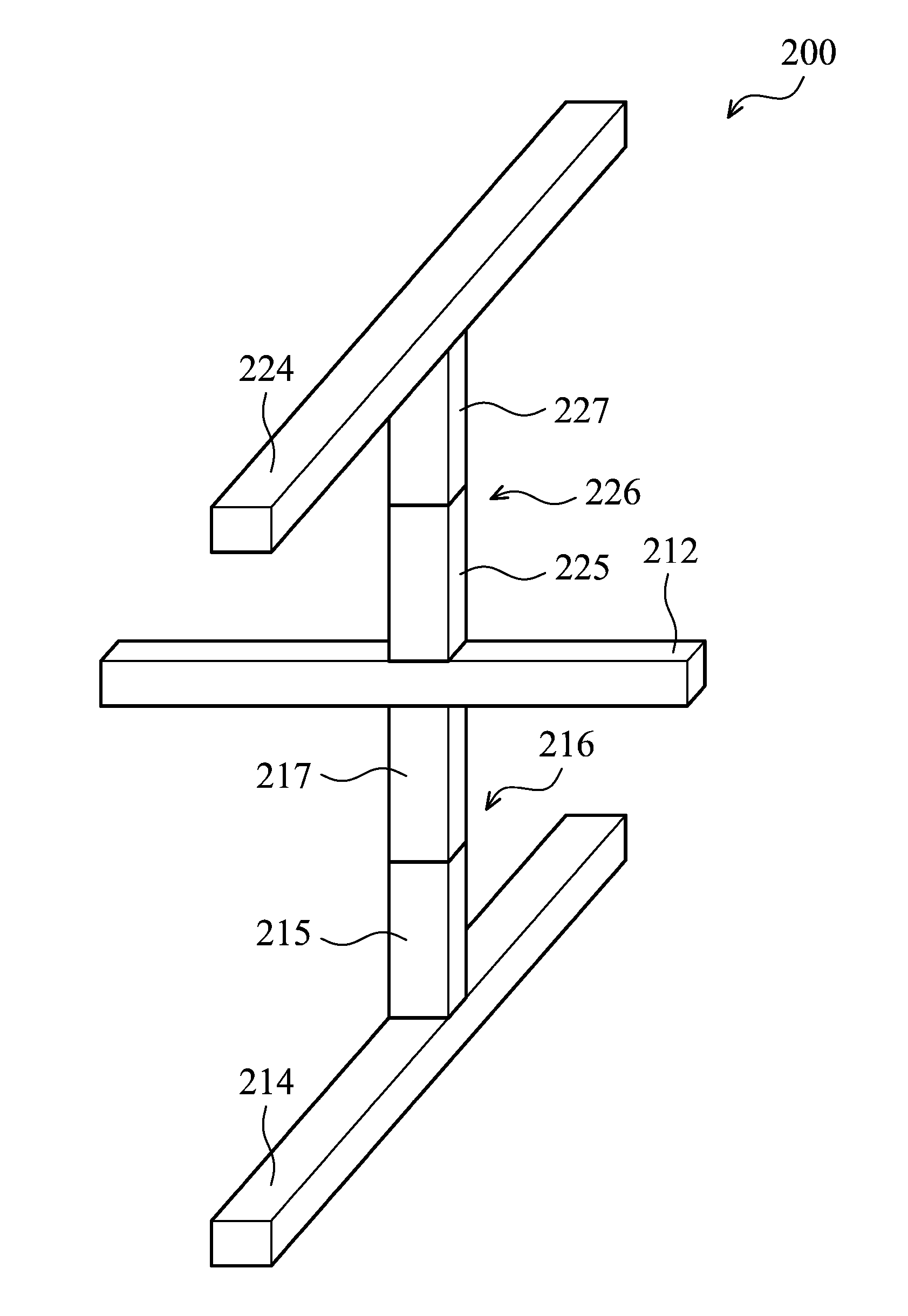
[0018]As key aspects and main features, embodiments of the invention provide a cross point memory array device. The cross point memory array with dual RRAM devic...


PUM


Abstract

Cross point memory arrays with CBRAM and RRAM stacks are presented. A cross point memory array includes a first group of substantially parallel conductive lines and a second group of substantially parallel conductive lines, oriented substantially perpendicular to the first group of substantially parallel conductive lines. An array of memory stack is located at the intersections of the first group of substantially parallel conductive lines and the second group of substantially parallel conductive lines, wherein each memory stack comprises a conductive bridge memory element in series with a resistive-switching memory element.

Description

BACKGROUND OF THE INVENTION[0001]1. Field of the Invention[0002]The invention relates to cross point memory array devices, and in particular, to a cross point memory array with memory stack including a conductive bridge memory element in series with a resistive-switching memory element.[0003]2. Description of the Related Art[0004]Conventional nonvolatile memories require three terminal MOSFET-based devices. The layout of such devices is not ideal, usually requiring feature sizes of 8f2 for each memory cell, where f is the minimum feature size. A cross point memory array such as a programmable metallization cell random access memory (PMCRAM) also known as a conductive bridge random access memory (CBRAM), a phase change memory (PCM), and a resistive random access memory (RRAM) are promising alternatives to conventional three terminal MOSFET-based devices, due to their smaller required feature sizes of 4f2 per cross points.[0005]U.S. Pat. No. 6,753,561, the entirety of which is hereby ...

Claims


Application Information

Patent Timeline
Patent Type & Authority Applications(United States)
IPC IPC(8): H01L47/00H01L29/12
CPCG11C13/0007G11C13/0011G11C13/003G11C2213/31G11C2213/75G11C2213/76H01L45/147H01L27/2463H01L27/2481H01L45/06H01L45/085H01L45/1233H01L45/146H01L27/2409H10B63/20H10B63/80H10B63/84H10N70/245H10N70/826H10N70/8833H10N70/8836
Inventor HSIEH, CHUN-IWU, CHANG-RONG
Owner NAN YA TECH
Why Eureka
Try Eureka