Spin-transfer multilayer stack containing magnetic layers with resettable magnetization

a multi-layer stack and magnetic layer technology, applied in the field of magnetic memory systems, can solve the problems of increasing physical area and complexity, increasing power consumption and heating, and affecting the density of memory cells at higher density

Inactive Publication Date: 2007-03-13
SAMSUNG SEMICON
View PDF9 Cites 288 Cited by
  • Summary
  • Abstract
  • Description
  • Claims
  • Application Information

AI Technical Summary

Benefits of technology

[0028]The present invention provides a spin-transfer stack device having a magnetization of the free layer that can be switched back and forth (and / or to any angle) using only the forward-bias switching mode, thereby minimizing the switching current density of a spin-transfer stack device. The present invention also provides a spin-transfer stack device that allows cell writing (i.e., switching) using a uni-directional current and using uni-directional elements, thereby decreasing process complexity, reducing cell size and / or enhancing performance. Additionally, the present invention provides a spin-transfer stack device capable of storing more than one bit per device (or cell), thereby increasing memory density.

Problems solved by technology

Although conventional magnetic memory 200 using conventional spin tunneling junctions 100′ can function, there are obstacles at higher memory cell densities.
This relatively large current can cause a host of problems in a conventional magnetic memory array 200, such as increased power consumption and heating.
The driving circuits required for driving the current that generates the switching field at a selected memory cell 220 also increase in physical area and complexity.
In conventional magnetic memory 200, the operation range for write current between the maximum and minimum values is small, resulting in reliability and consistency problems.
The high current density that is required for producing the spin-transfer effect in a conventional spin tunneling junction, however, could destroy its thin insulating barrier due to ohmic dissipation.
Thus, it may be impossible to use the spin-transfer effect for writing to a magnetic memory consisting of conventional spin tunneling junction magnetic elements 100′.
The single-spacer spin-transfer stack type suffers numerous disadvantages, including an extremely small signal, a low resistance, and a high switching current.
The single-barrier and dual-barrier spin-transfer stack devices suffer from numerous disadvantages, including an extremely high resistance, a high switching current, an unreliable method of fabrication, and a lack of working experimental evidence of spin-transfer effect switching across tunnel barrier(s) at room temperature.
The low-resistance tunnel barrier significantly increases the read signal, but yet keeps the total stack resistance low.

Method used


Image

  • Spin-transfer multilayer stack containing magnetic layers with resettable magnetization
  • Spin-transfer multilayer stack containing magnetic layers with resettable magnetization
  • Spin-transfer multilayer stack containing magnetic layers with resettable magnetization

Examples


Embodiment Construction

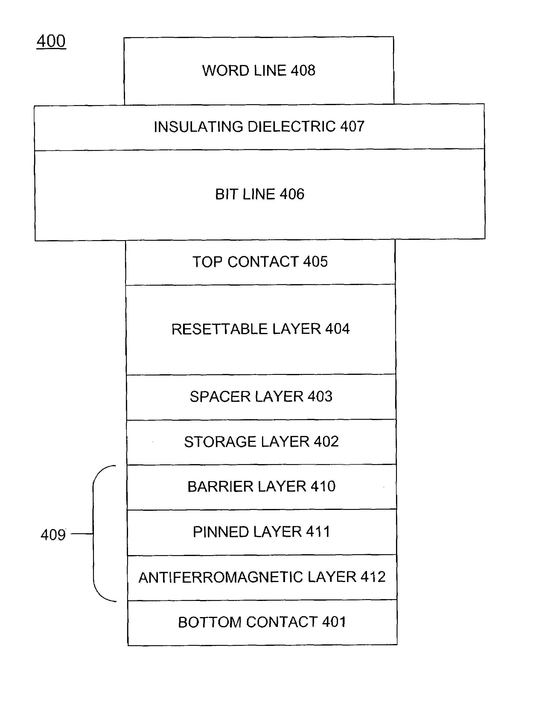
[0053]The present invention provides a spin-transfer stack device having a magnetization of the free or storage layer that can be switched back and forth (and / or to any angle) using only the forward-bias switching mode, thereby minimizing the switching current density of a spin-transfer stack device. The present invention also provides a spin-transfer stack device that allows cell writing (i.e., switching) using a uni-directional current and using uni-directional elements, thereby decreasing process complexity, reducing cell size and / or enhancing performance. Additionally, the present invention provides a spin-transfer stack device capable of storing more than one bit per device (or cell), thereby increasing memory density.

[0054]The present invention provides a spin-transfer stack device having a pinned layer, referred to herein as a “resettable” layer, that is ferromagnetic, ferrimagnetic or sperimagnetic. The magnetization of the resettable layer should easily be set in a desired ...


PUM


Abstract

A magnetic element for a high-density memory array includes a resettable layer and a storage layer. The resettable layer has a magnetization that is set in a selected direction by at least one externally generated magnetic field. The storage layer has at least one magnetic easy axis and a magnetization that changes direction based on the spin-transfer effect when a write current passes through the magnetic element. An alternative embodiment of the magnetic element includes an additional multilayer structure formed from a tunneling barrier layer, a pinned magnetic layer and an antiferromagnetic layer that pins the magnetization of the pinned layer in a predetermined direction. Another alternative embodiment of the magnetic element includes an additional multilayer structure that is formed from a tunneling barrier layer and a second resettable layer having a magnetic moment that is different from the magnetic moment of the resettable layer of the basic embodiment.

Description

BACKGROUND OF THE INVENTION[0001]1. Field of the Invention[0002]The invention relates to magnetic memory systems. More particularly, the present invention relates to a method and system for providing an element that employs a spin-transfer effect in switching and that can be used in a magnetic memory, such as a magnetic random access memory (“MRAM”).[0003]2. Description of the Related Art[0004]Magnetic memories are used for storing data. One type of memory element of interest utilizes magnetoresistance properties of a magnetic element for storing data. FIGS. 1A and 1B respectively depict cross sectional views of a conventional spin valve magnetic element 100 and a conventional spin tunneling junction magnetic element 100′. As shown in FIG. 1A, conventional spin valve magnetic element 100 includes a conventional antiferromagnetic (AFM) layer 102, a conventional pinned layer 104, a conventional spacer layer 106, and a conventional free layer 108. Conventional pinned layer 104 and conv...

Claims


Application Information

Patent Timeline
Patent Type & Authority Patents(United States)
IPC IPC(8): G11C11/00H01L43/00G11C11/15
CPCG11C11/5607G11C11/15
Inventor NGUYEN, PAUL P.HUAI, YIMING
Owner SAMSUNG SEMICON
Why Eureka
Try Eureka