Solid-State Image Sensor and Drive Method for the Same

a solid-state image sensor and drive method technology, applied in the field of solid-state image sensors and drive methods, can solve the problems of limited number of storage ccds that can be mounted on a single sensor, difficulty in aforementioned in-situ storage image sensors, and limited frame availability for aforementioned high-speed imaging, etc., to achieve low cost, high usability, and low cost

Active Publication Date: 2011-04-14
TOHOKU UNIV +1
View PDF10 Cites 29 Cited by
  • Summary
  • Abstract
  • Description
  • Claims
  • Application Information

AI Technical Summary

Benefits of technology

[0034]The solid-state image sensor and its drive method according to the present invention make it possible to concurrently perform both an ultrahigh-speed imaging operation (e.g. at one million frames per second or higher) and a rather slow but long-time repetitive imaging operation by only one image sensor. Thus, one can provide an imaging device that is relatively inexpensive yet w

Problems solved by technology

However, the number of storage CCDs that can be mounted on a single sensor is limited due to various factors, such as the limited area of a semiconductor chip and the restriction on power consumption.
Accordingly, the number of frames available for the aforementioned high-speed imaging is limited.
It is difficult for the aforementioned in-situ storage image sensor to meet the demands for such imaging.
Such an imaging system will be expensive.
However, in some situations, it

Method used


Image

  • Solid-State Image Sensor and Drive Method for the Same
  • Solid-State Image Sensor and Drive Method for the Same
  • Solid-State Image Sensor and Drive Method for the Same

Examples


Embodiment Construction

[0047]A solid-state image sensor and its drive method, which are an embodiment of the present invention, are hereinafter described with reference to the attached drawings.

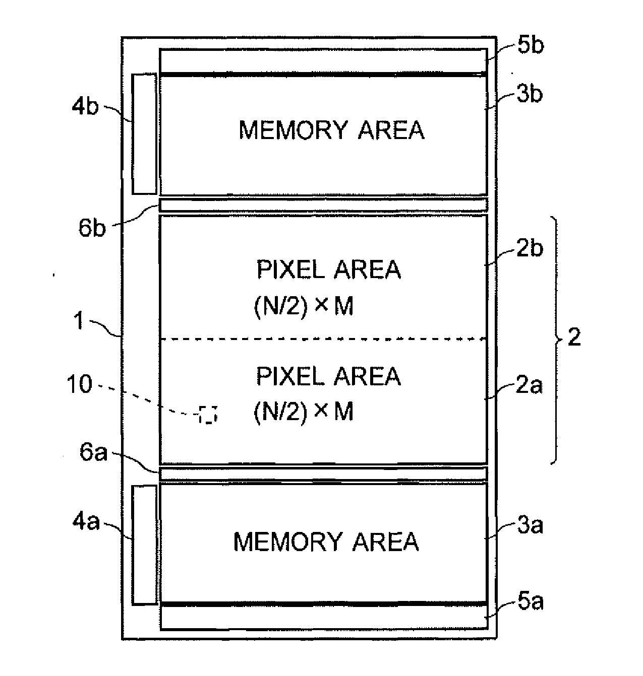
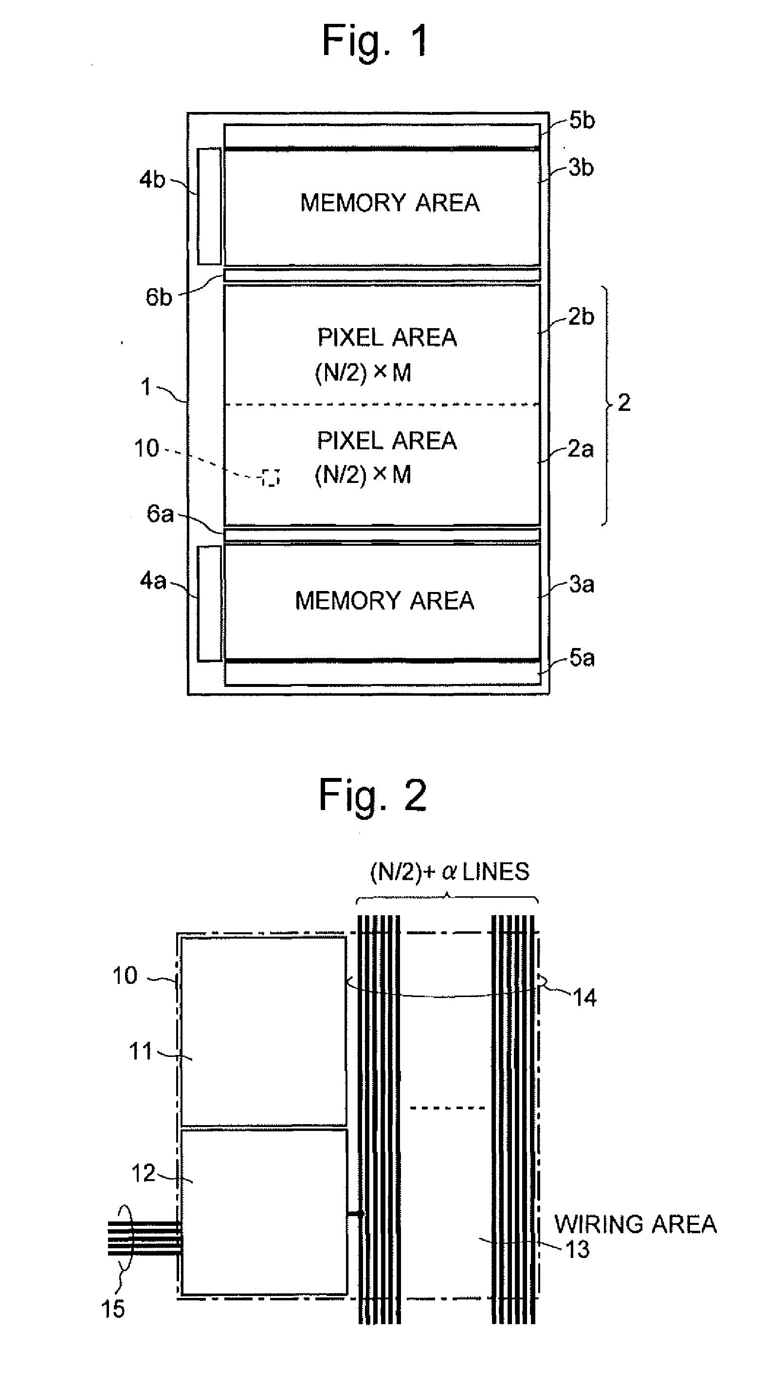
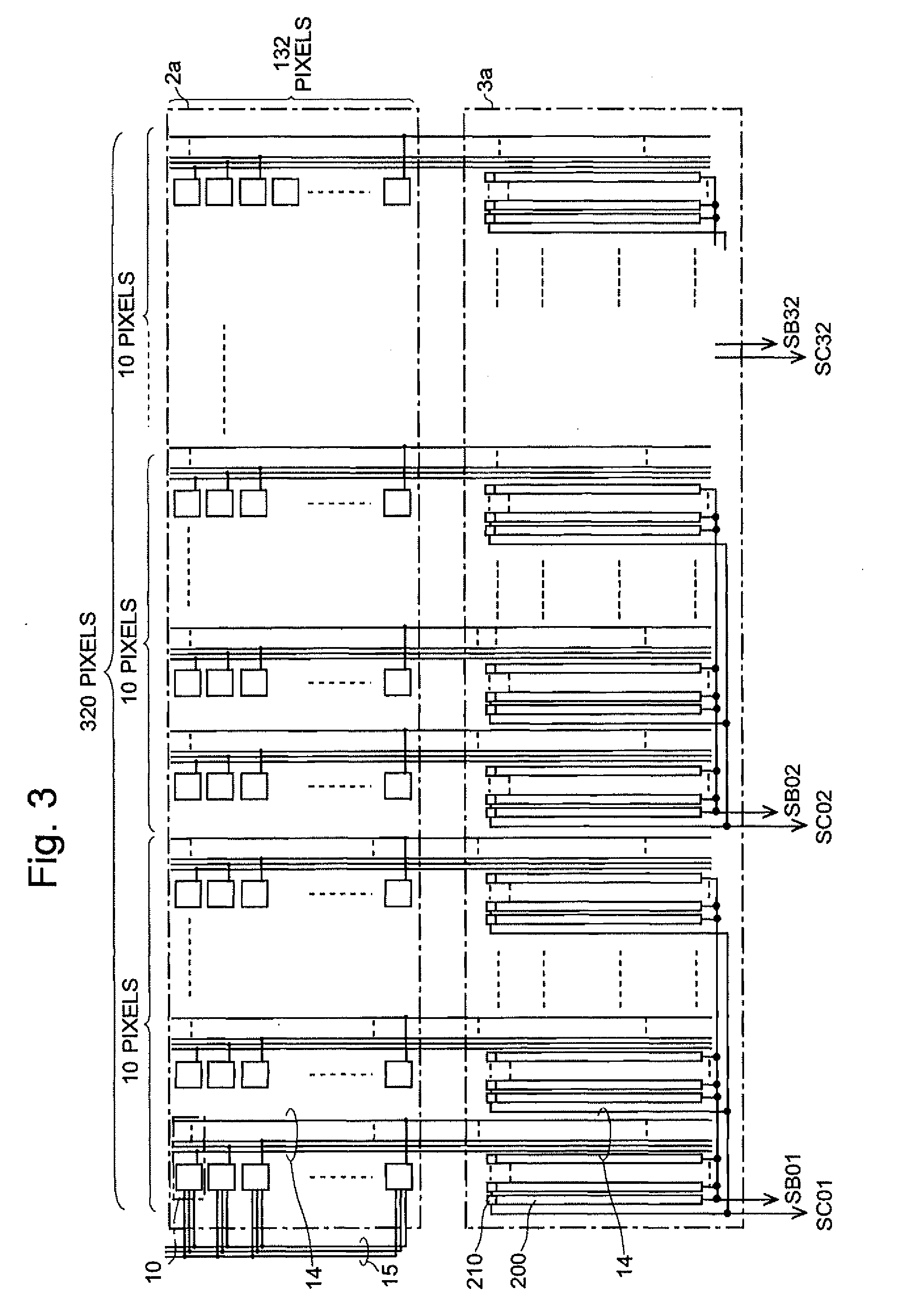
[0048]The overall circuit configuration and structure of the solid-state image sensor according to the present embodiment is described by means of FIGS. 1-4. FIG. 1 is a schematic plan view showing the layout on a semiconductor chip of a solid-state image sensor according to the present embodiment. FIG. 2 is a schematic plan view showing the layout of one pixel within a pixel area shown in FIG. 1. FIG. 3 is a plan view showing a schematic configuration of the pixel area and the memory area. FIG. 4 is a schematic circuit configuration diagram of one pixel and a corresponding memory section.

[0049]The solid-state image sensor includes a semiconductor substrate 1, on which a pixel area 2 for receiving incident light and producing pixel signals for each pixel as well as two memory areas 3a and 3b for holding pixel signa...


PUM


Abstract

A burst reading memory section (200) and continuous reading memory section (210) are independently provided for each of the two-dimensionally arrayed pixels (10). The burst reading memory section (200) has capacitors (25001-25104) capable of holding a plurality of signals. The continuous reading memory section (210) has only one capacitor 213. Signal output lines for the two memory sections are separately provided. When a signal produced by photoelectric conversion at the pixel (10) is outputted on a pixel output line (14), the signal can be simultaneously written in the capacitors at both memory sections (200, 201), after which the signals can be separately extracted to the outside at different timings. Therefore, a series of images taken at extremely short intervals of time during a short period of time can be obtained at an arbitrary timing without impeding a continuous image-acquiring operation at a low frame rate. Accordingly, both an ultrahigh-speed imaging operation having a limitation on the number of frames and an imaging that is rather slow but has no limitation on the number of frames can be simultaneously performed.

Description

TECHNICAL FIELD[0001]The present invention relates to a solid-state image sensor and a drive method for this sensor. More specifically, it relates to a solid-state image sensor capable of high-speed operations suitable for taking images of high-speed phenomena, such as destructions, explosions or combustions, and a drive method for such a sensor.BACKGROUND ART[0002]High-speed imaging devices (high-speed video cameras) used for taking consecutive images of high-speed phenomena, such as explosions, destructions, combustions, collisions or discharges, for only a short period of time have been conventionally developed (for example, refer to Non-Patent Document 1 and other documents). Such high-speed imaging devices need to perform an ultrahigh-speed imaging operation that exceeds a level of approximately one million frames per second. Accordingly, they use solid-state image sensors capable of high-speed operations, which have special structures different from those of the conventional i...

Claims


Application Information

Patent Timeline
IPC IPC(8): H04N5/335H04N5/357H04N5/378
CPCH04N5/37452H04N5/378H04N5/3575H01L27/14843H04N25/616H04N25/771H04N25/75
Inventor SUGAWA, SHIGETOSHIKONDO, YASUSHITOMINAGA, HIDEKI
Owner TOHOKU UNIV
Why Eureka
Try Eureka