Method and system for exposing delicate structures of a device encapsulated in a mold compound

a technology of mold compound and delicate structure, which is applied in the direction of solid-state devices, manufacturing tools, welding/soldering/cutting articles, etc., can solve the problems of preventing access to these specific ic structures, physical access to interior points may also be needed, and failure of integrated circuits

Inactive Publication Date: 2011-04-21
CONTROL LASER
View PDF15 Cites 2 Cited by
  • Summary
  • Abstract
  • Description
  • Claims
  • Application Information

AI Technical Summary

Problems solved by technology

Integrated circuits fail.
However, once they fail, it is often necessary to determine what causes such failure as it may trigger a product recall leading to corrective action.
Additionally, physical access to interior points may also be needed to isolate problems.
However, access to these specific IC structures is prevented by the protective encapsulated mold compound.
Although the prior art solution has been satisfactory, it suffers from the disadvantage that it cannot adequately ablate some resin compounds which utilize glass or silicon fillers which are too large or too numerous.
Raising the power of the beam sufficient to overcome the energy loss as a result of the diffusion will result in destruction of the sensitive IC components where the beam is not diffused, destroying or damaging the IC chip to a point where failure analysis cannot be performed.

Method used


Image

  • Method and system for exposing delicate structures of a device encapsulated in a mold compound
  • Method and system for exposing delicate structures of a device encapsulated in a mold compound
  • Method and system for exposing delicate structures of a device encapsulated in a mold compound

Examples


Embodiment Construction

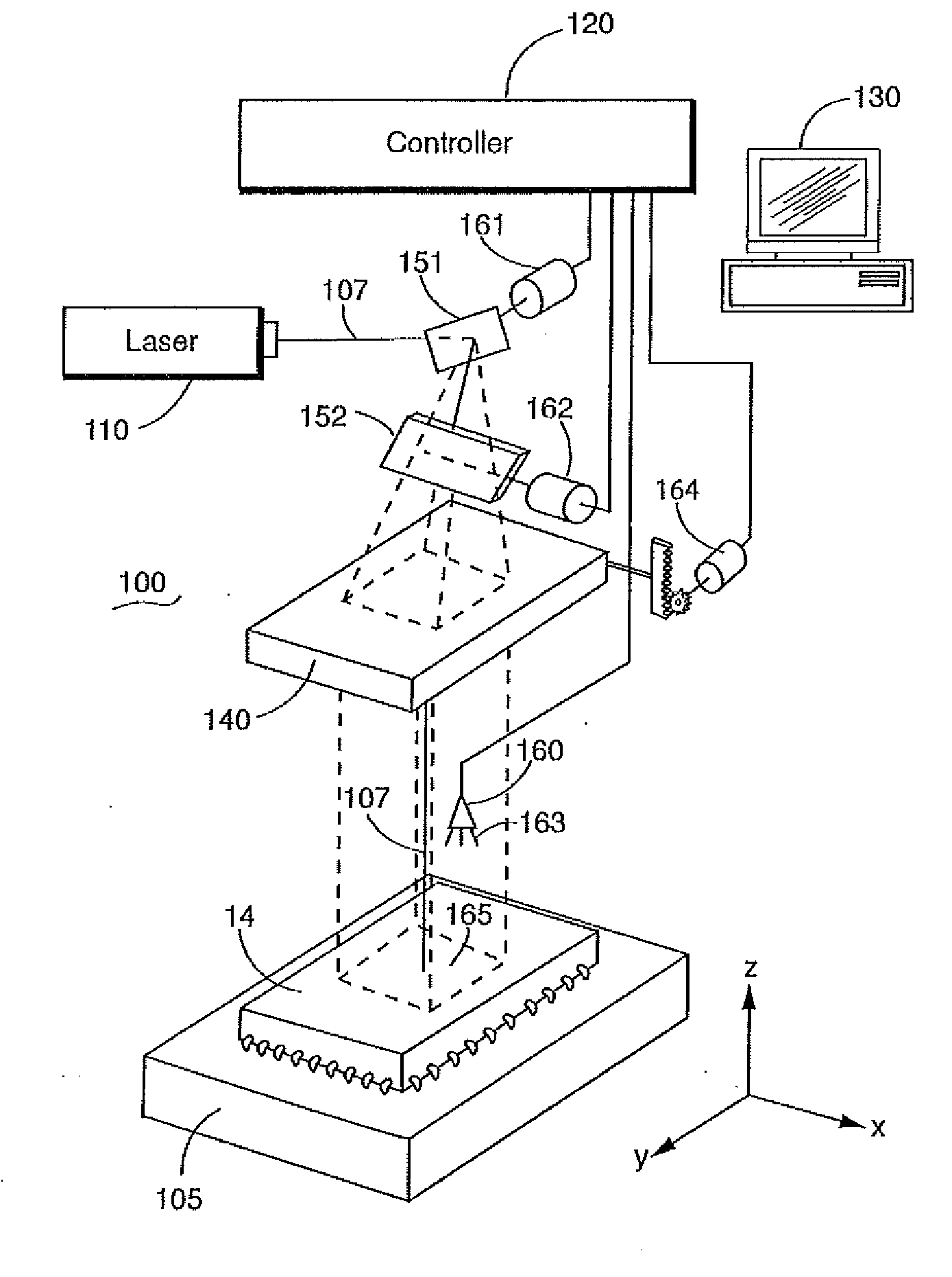
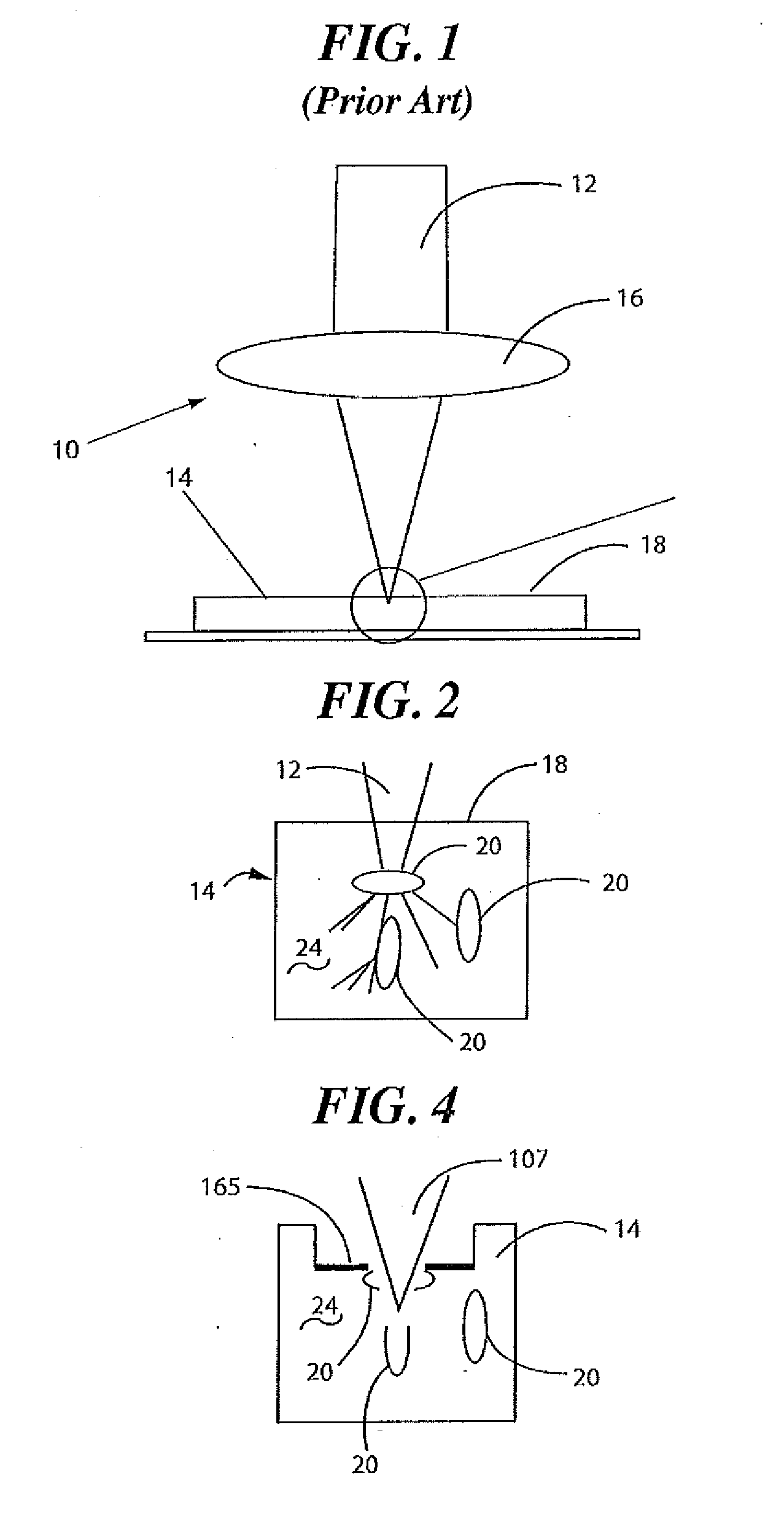
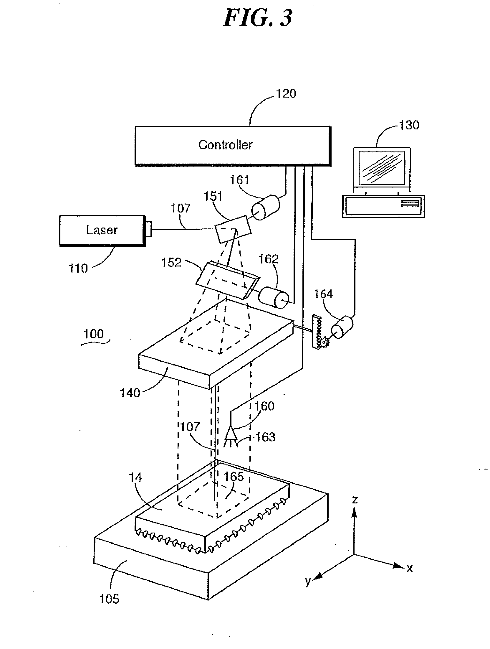
[0013]FIG. 3 is a block diagram of an exemplary embodiment of a system 100 in accordance with the present invention. A device to be analyzed, such as an integrated circuit (IC) 14, is placed on a platform 105 upon which a laser beam 107 generated by a laser 110 is steered and focused by a pair of reflective paddles 151 and 152 and a lens element 140. Operation is controlled by a controller 120 which may be coupled to a user interface 130 for human interaction. For example, the controller 120 and user interface 130 may be part of a workstation, personal computer or the like or may be housed separately.

[0014]During operation, the IC 14 is stationary as the beam 107 is moved over a selected portion of the surface of the IC in a selected pattern. At any one instant, the laser beam 107 impinges on one point on the surface of the IC 101. To the human eye, however, the beam may appear as a line or as a rectangle on the surface of the IC 101, depending on how fast the beam 107 is steered ov...


PUM

PropertyMeasurementUnit
wavelengthaaaaaaaaaa
speedsaaaaaaaaaa
wavelengthsaaaaaaaaaa

Abstract

A system utilizes a laser to remove the mold compound of an IC without damaging the internal die, wire leads, solder connections and any other critical structures encapsulated within the mold compound, thereby leaving them available for the provisional and electrical analysis. A laser beam is focused through appropriate optics onto a plane corresponding to the surface of an IC. A layer of material which is opaque at the wave length of the laser beam is applied at the surface of the IC chip to be ablated prior to each pass of the laser. A spray nozzle may be provided to move in synchronous motion ahead of the laser being to apply coat of the opaque material.

Description

BACKGROUND OF THE INVENTION[0001]The present invention relates to methods and systems for using an ablating laser in preparing an integrated circuit for failure analysis, in particular, for preparing an electrical device or circuitry having components encapsulated in a mold compound containing a glass or silicon impurities.[0002]Integrated circuits fail. However, once they fail, it is often necessary to determine what causes such failure as it may trigger a product recall leading to corrective action. In failure analysis, each component of the integrated circuit is tested to determine whether that particular element is the cause of the failure. The basic structure of the typical integrated circuit (IC) includes a rectangular, semiconductor die or chip surrounded by and connected to a number of fine wire leads which are further connected to a surrounding frame of thicker metallic traces which in turn form the external pins of the IC. With the exception of the external pins, the entir...

Claims


Application Information

Patent Timeline
Patent Type & Authority Applications(United States)
IPC IPC(8): B23K26/00
CPCB23K26/0807B23K26/1411B23K26/1417B23K26/4085H01L21/56H01L2924/0002B23K26/009H01L2924/00B23K26/40B23K26/082B23K26/144B23K26/146B23K2103/16
Inventor ANDERSON, GREGORY B.
Owner CONTROL LASER
Why Eureka
Try Eureka