

Mictostrip transmission line structure with vertical stubs for reducing far-end crosstalk
- Summary
- Abstract
- Description
- Claims
- Application Information
AI Technical Summary
Benefits of technology
Problems solved by technology
Method used
Image

Examples
first embodiment
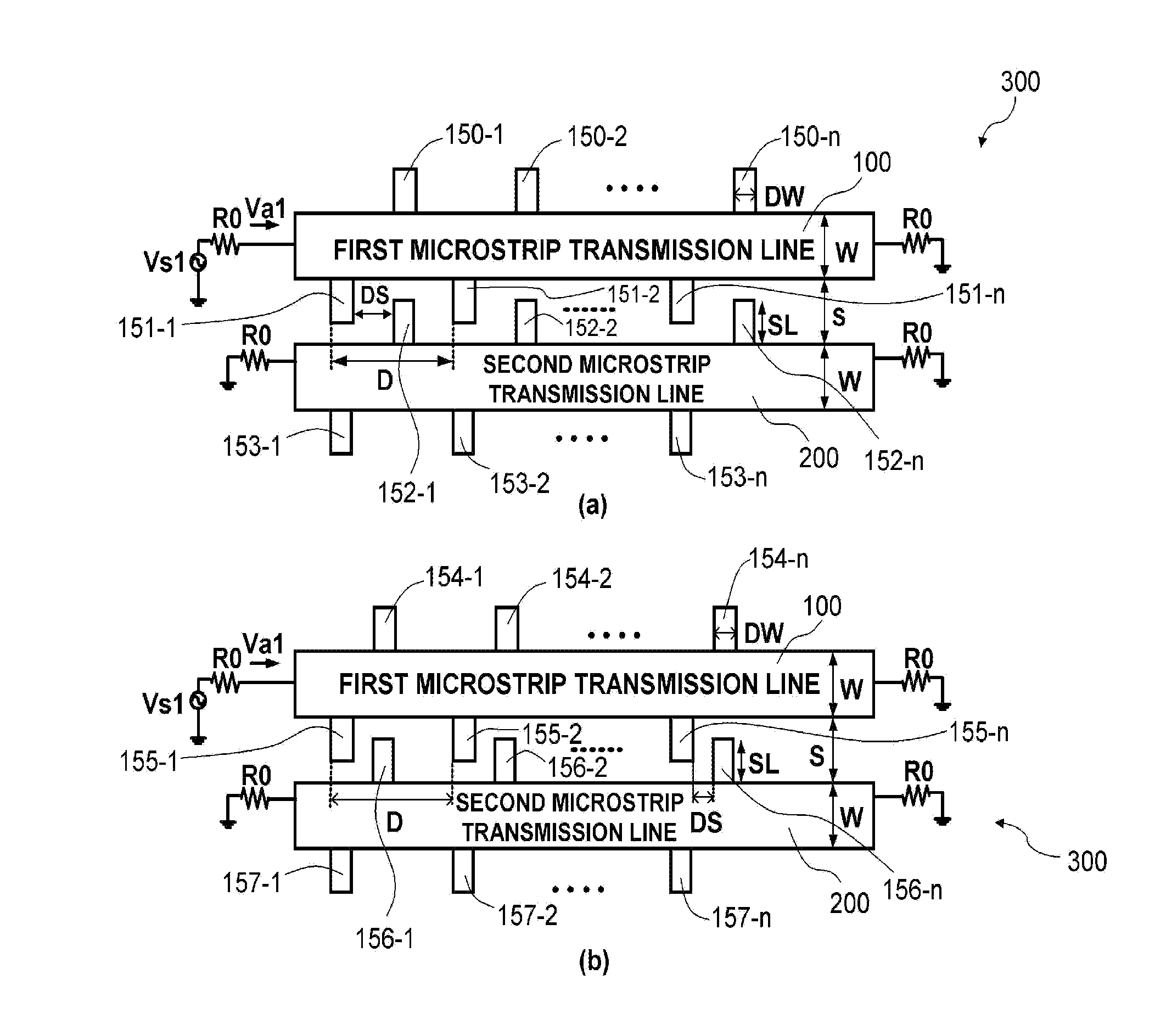
[0043]According to the present invention illustrated in FIG. 4a, the second stubs 151-1 to 151-n formed at the first microstrip transmission line 100 and the third stubs 152-1 to 152-n formed at the second microstrip transmission line 200 do not face each other at the same positions in the length directions of the first and second microstrip transmission lines 100 and 200 but are disposed in alternate positions in the length directions of the first and second microstrip transmission lines 100 and 200.
[0044]In addition, the fourth stubs 153-1 to 153-n are disposed at the second microstrip transmission line 200 to extend in such a direction to be far from the first microstrip transmission line 100. Here, the fourth stubs 153-1 to 153-n may be disposed at the same positions in the length direction of the transmission line as the second stubs 151-1 to 151-n that are disposed at the first microstrip transmission line 100 to face the second microstrip transmission line 200. Namely, the se...
second embodiment
[0048]According to the present invention as illustrated in FIG. 4b, an arrangement of the fifth to eighth stubs 154-1 to 154-n, 155-1 to 155-n, 156-1 to 156-n, and 157-1 to 157-n is similar to that of the first to fourth stubs 150-1 to 150-n, 151-1 to 151-n, 152-1 to 152-n, and 153-1˜153-n described above. The seventh stubs 156-1 to 156-n that are formed at the second microstrip transmission line 200 are disposed to be adjacent to the sixth stubs 155-1 to 155-n formed at the first microstrip transmission line 100 at minimum intervals which are allowed in a manufacturing process in the length direction of the transmission line. A bundle structure including one of the sixth stubs 155-1 to 155-n and one of the seventh stubs 156-1 to 156-n as a bundle is uniformly repeated in the length direction of the transmission line.
[0049]Here, the transmission line length direction distance DS is determined so that a difference between a capacitive coupling ratio and an inductive coupling ratio is...
third embodiment
[0062]In addition, according to the present invention illustrated in FIG. 9, a third microstrip transmission line 250 which is disposed at a side of the first microstrip transmission line 100 to be parallel thereto in the opposite direction to the second microstrip transmission line 200 is further included.
[0063]A number of stubs formed at the third microstrip transmission line 250 may be disposed at predetermined intervals as illustrated in FIG. 4a or disposed so that the stubs 158-1 to 158-n and 159-1 to 159-n have minimum intervals as illustrated in FIG. 4b. As described above, the microstrip transmission line structure with the vertical stubs according to the present invention may be extended by adding the transmission lines and the stubs.
[0064]Simulation results using the microstrip transmission line structure with the vertical stubs for reducing the far-end crosstalk according to the present invention are described.
[0065]According to the present invention, by using a self-indu...
PUM
 Abstract
Description
Claims
Application Information