Developing apparatus, developing method and storage medium

a technology of developing apparatus and developing method, which is applied in the field of developing method and storage medium, can solve the problems of increasing increasing the degree of defective development, and reducing the difficulty of uniformly spreading a developer, so as to achieve high water repellency and reduce the effect of development defects

Active Publication Date: 2011-04-28
TOKYO ELECTRON LTD
View PDF6 Cites 19 Cited by
  • Summary
  • Abstract
  • Description
  • Claims
  • Application Information

AI Technical Summary

Benefits of technology

[0007]The present invention has been made under such circumstances and it is therefore an object of the present invention to provide a developing apparatus and a developing method capable of highly uniformly processing the surface of a substrate processed by an exposure process even if the surface has high water repellency and of reducing developing defects that are created by the developing process, and a storage medium for storing the program of the developing method.
[0014]The developing apparatus of the present invention that wets the substrate with the developer forms a puddle of the diffusion-assisting liquid not having any developing effect on the central part of the substrate, spouts the developer onto the central part of the substrate being rotated in the normal direction, and then rotates the substrate for prewetting. The developer is born on the diffusion-assisting liquid and spreads all over the surface of the substrate with the assistance of the diffusion-assisting liquid. Consequently, dissolvable patterning parts of the resist film dissolve and adhere to nonpatterning parts of the resist film. Thus, contact angle between the developer and the surface of the substrate equivalent to the degree of repellency is small, and it is easy for the developer to spread uniformly all over the surface of the substrate for development. Consequently, the entire surface of the substrate can be highly uniformly processed for development and development defects can be reduced even if the surface of the exposed substrate has high water repellency.

Problems solved by technology

However, the high water repellency of the surface of the wafer enhances difficulty in uniformly spreading a developer over the surface of the wafer in a developing process.
Consequently, it is possible that the degree of defective development increases with the further minimization of the minimum feature size of patterns.
If the surface of the wafer has high water repellency, it is difficult to spread the developer uniformly particularly in a circumferential part of the surface and the above-mentioned problems cannot be solved.

Method used


Image

  • Developing apparatus, developing method and storage medium
  • Developing apparatus, developing method and storage medium
  • Developing apparatus, developing method and storage medium

Examples


Embodiment Construction

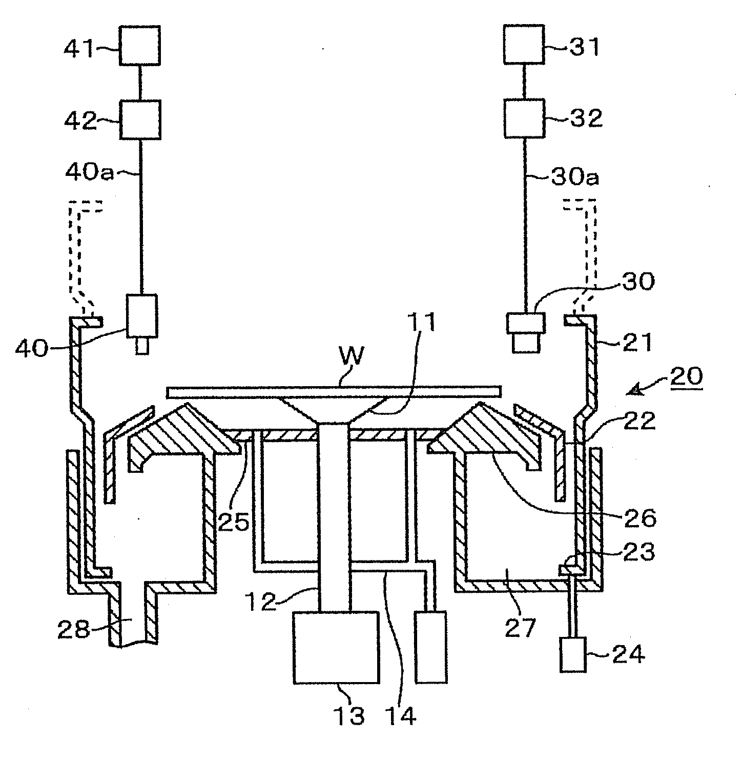
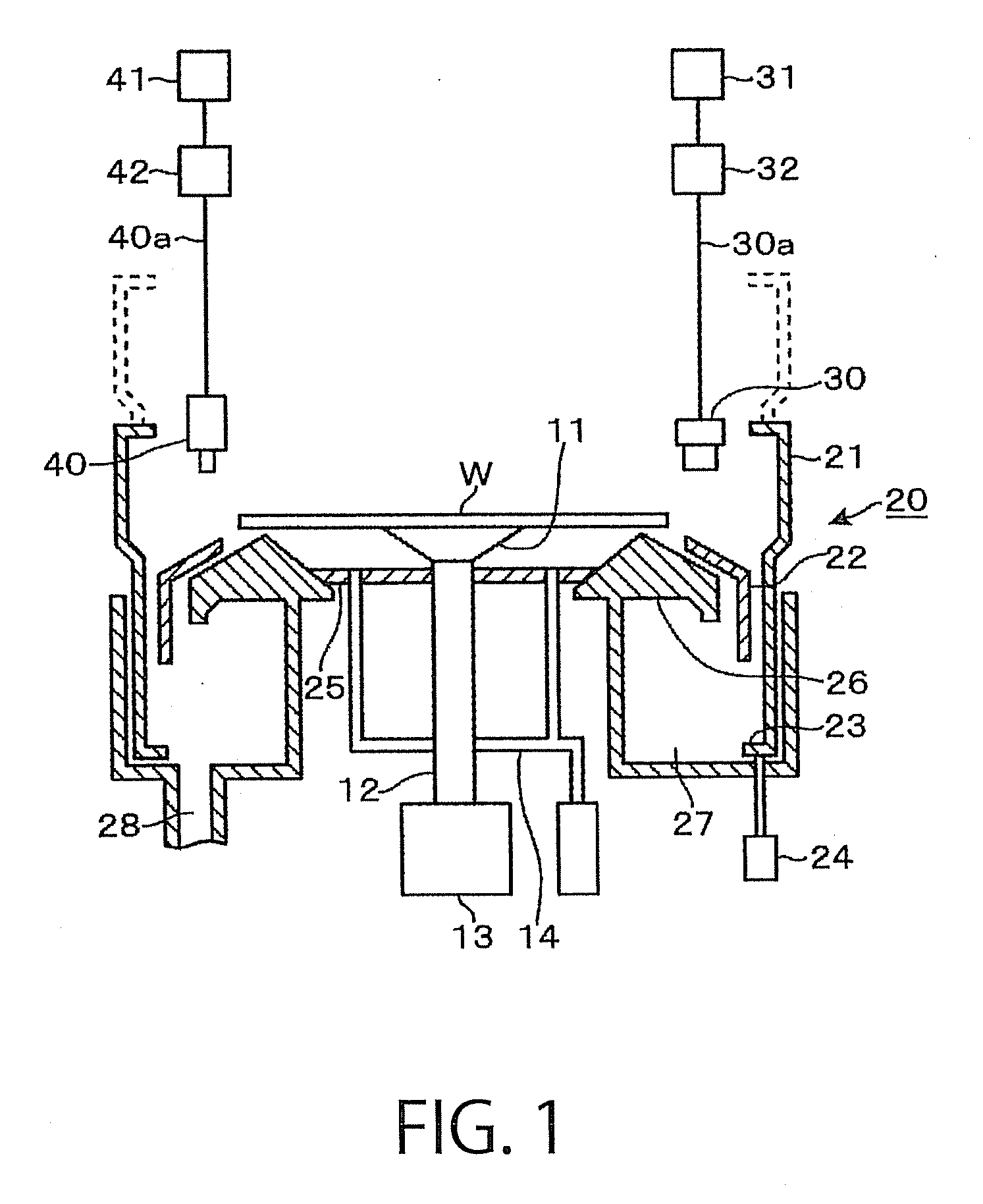
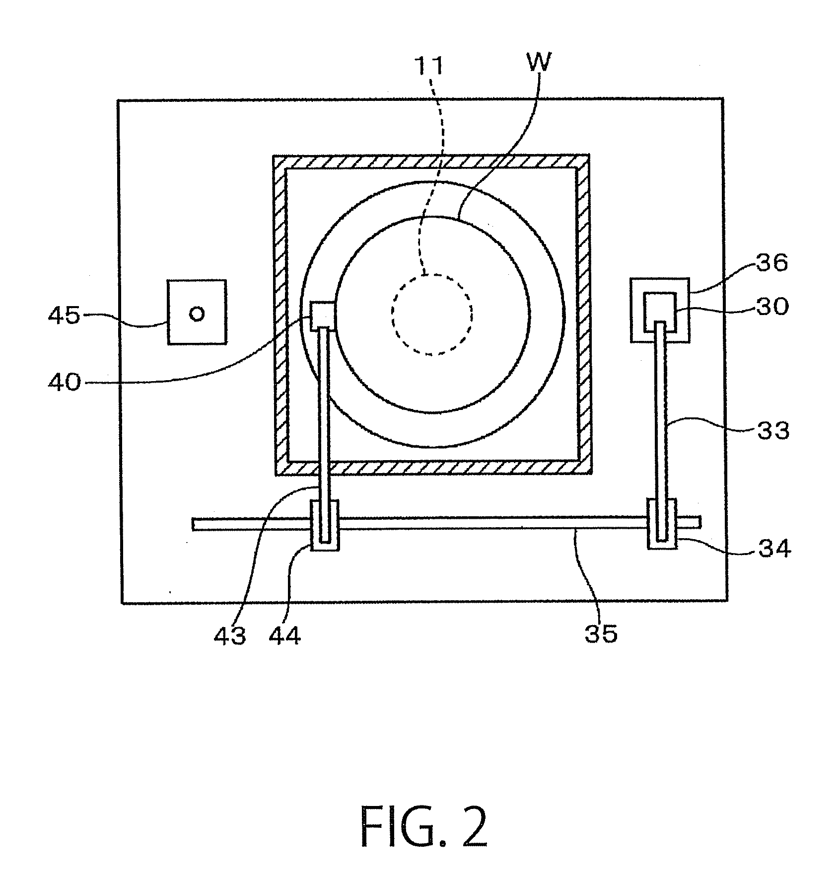
[0024]Referring to FIGS. 1 and 2 showing a developing apparatus in a preferred embodiment according to the present invention, the developing apparatus is provided in its central part with a spin chuck 11, namely, a substrate holding device, for holding a wafer W, namely, a substrate, by suction. The spin chuck 11 is connected to a rotational drive unit 13 including, for example, a motor, by a drive shaft 12. The rotational drive unit 13 is disposed under the spin chuck 11. The spin chuck 11 can be vertically moved by a lifting mechanism incorporated into the rotational drive unit 13. The rotational drive unit 13 can rotate the drive shaft 12 in the normal and the reverse direction. Normal rotation and reverse rotation do not necessarily correspond to clockwise rotation and counterclockwise rotation, respectively. Either of clockwise rotation and counterclockwise rotation and the other rotation may be used to describe rotating the wafer sequentially in opposite directions for conveni...


PUM


Abstract

A pretreatment process, carried out prior to a developing process, spouts pure water, namely, a diffusion-assisting liquid for assisting the spread of a developer over the surface of a wafer, through a cleaning liquid spouting nozzle onto a central part of the wafer to form a puddle of pure water. The developer is spouted onto the central part of the wafer for prewetting while the wafer is rotated at a high rotating speed to spread the developer over the surface of the wafer. The developer dissolves the resist film partly and produces a solution. The rotation of the wafer is reversed, for example, within 7 s in which the solution is being produced to reduce the water-repellency of the wafer by spreading the solution over the entire surface of the wafer. Then, the developer is spouted onto the rotating wafer to spread the developer on the surface of the wafer.

Description

BACKGROUND OF THE INVENTION[0001]1. Technical Field[0002]the present invention relates to techniques for processing a substrate coated with a resist film and processed by an exposure process for development by a developing process.[0003]2. Background Art[0004]A photoresist pattern forming process, namely, one of semiconductor device fabricating processes, forms a resist film on a surface of a semiconductor wafer (hereinafter, referred to simply as “wafer”), exposes the resist film to light in a predetermined pattern, and then develops the exposed resist film by a developing process using a developer to form a resist pattern. A known developing process mentioned in JP-A 2006-60084 holds a wafer by a spin chuck, namely, a substrate holding device, spouts a developer onto the wafer through a developer spouting nozzle moving from a position above the circumference of the wafer toward a position above the center of the wafer while the wafer is rotated about a vertical axis.[0005]A known ...

Claims


Application Information

Patent Timeline
Patent Type & Authority Applications(United States)
IPC IPC(8): G03B27/52G03D3/00
CPCG03F7/3021
Inventor TAKEGUCHI, HIROFUMIISEKI, TOMOHIROYOSHIDA, YUICHIYOSHIHARA, KOUSUKE
Owner TOKYO ELECTRON LTD
Why Eureka
Try Eureka