Power supply apparatus
a technology of power supply apparatus and film thickness distribution, which is applied in the direction of vacuum evaporation coating, plasma technique, coating, etc., can solve the problems of difficult to detect anomalous electric discharge (arcing) when it occurs, and achieve the effect of easy to achieve uniform film thickness distribution
- Summary
- Abstract
- Description
- Claims
- Application Information
AI Technical Summary
Benefits of technology
Problems solved by technology
Method used
Image


Examples
Embodiment Construction
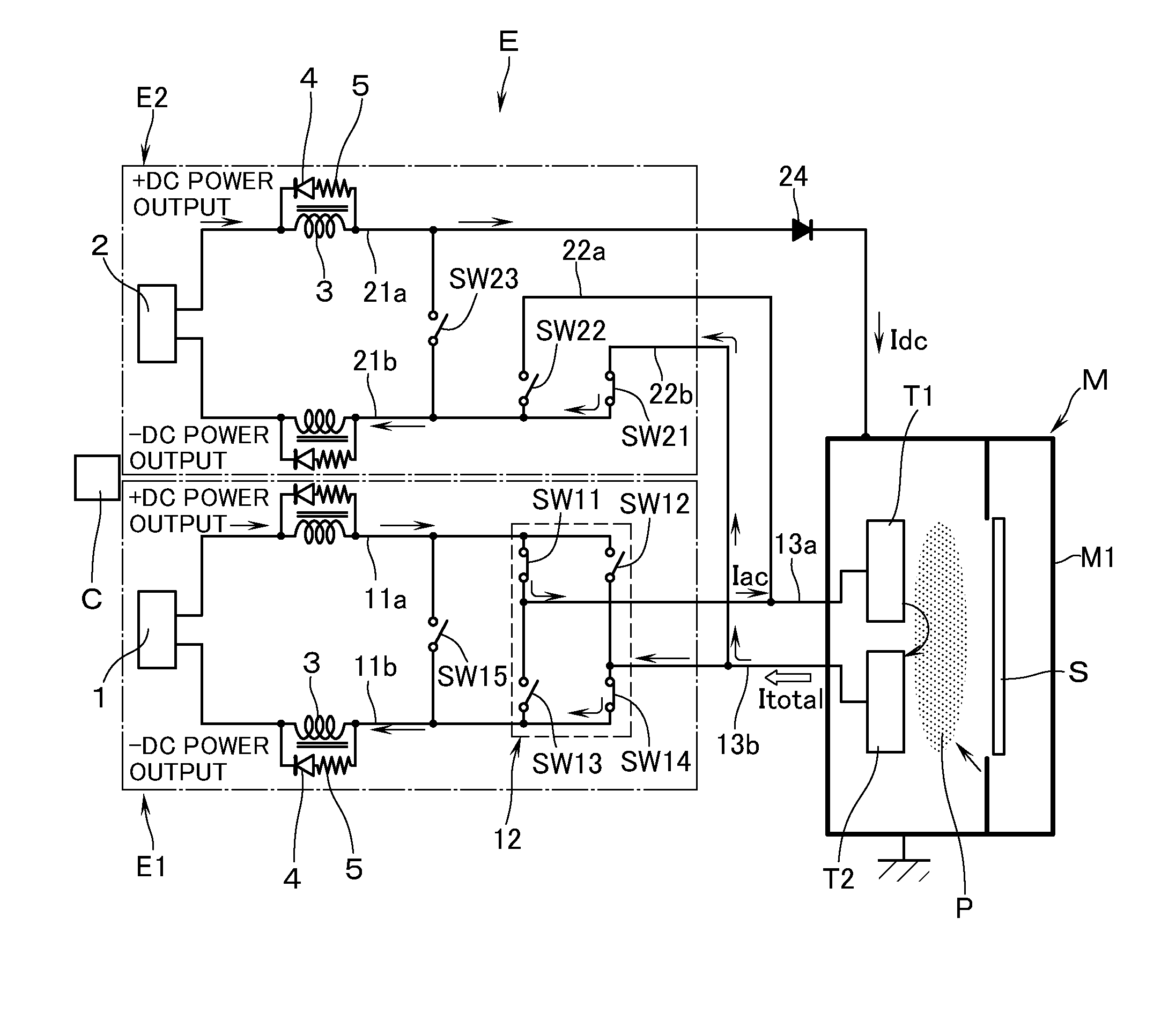
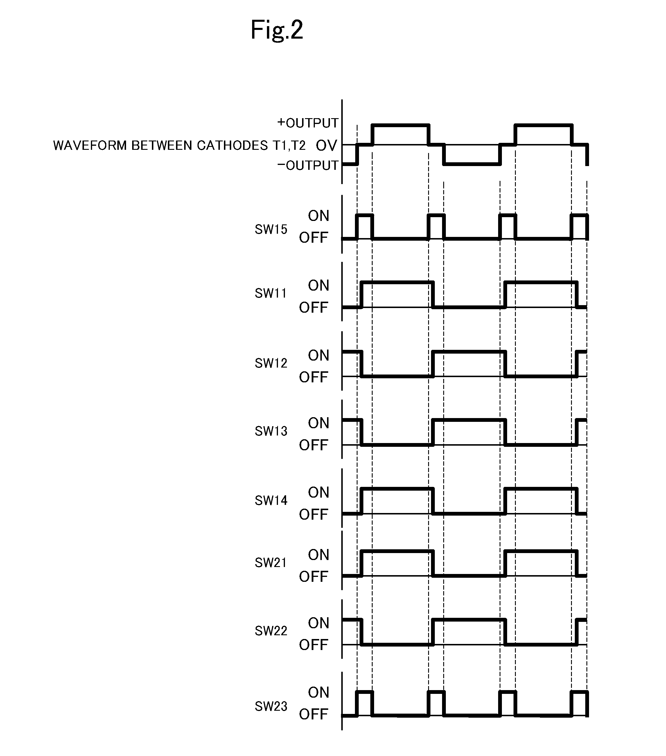
[0016]With reference to the accompanying drawings a description will now be made of a power supply apparatus E according to an embodiment of this invention. The power supply apparatus E is used to charge (output) a pair of targets T1, T2, which serve as electrodes to come into contact with a plasma P, with AC pulsed power at a predetermined frequency, the targets T1, T2 being disposed opposite to a substrate S which is to be processed and is present inside a vacuum chamber M1, e.g., of a sputtering apparatus M. The power supply apparatus E is. The power supply apparatus E has: a first discharge circuit E1 and a second discharge circuit E2; and a control means C which centrally controls the operation, and the like of switching elements (to be described hereinafter) which are disposed in the first discharge circuit E1 and the second discharge circuit E2 (see FIG. 1).
[0017]The first discharge circuit E1 has a DC power supply source 1 which enables the supply of DC power. The DC power s...
PUM
| Property | Measurement | Unit |
|---|---|---|
| frequency | aaaaa | aaaaa |
| frequency | aaaaa | aaaaa |
| frequency | aaaaa | aaaaa |
Abstract
Description
Claims
Application Information