

Method for manufacturing light-emitting diode
- Summary
- Abstract
- Description
- Claims
- Application Information
AI Technical Summary
Benefits of technology
Problems solved by technology
Method used
Image

Examples
first embodiment
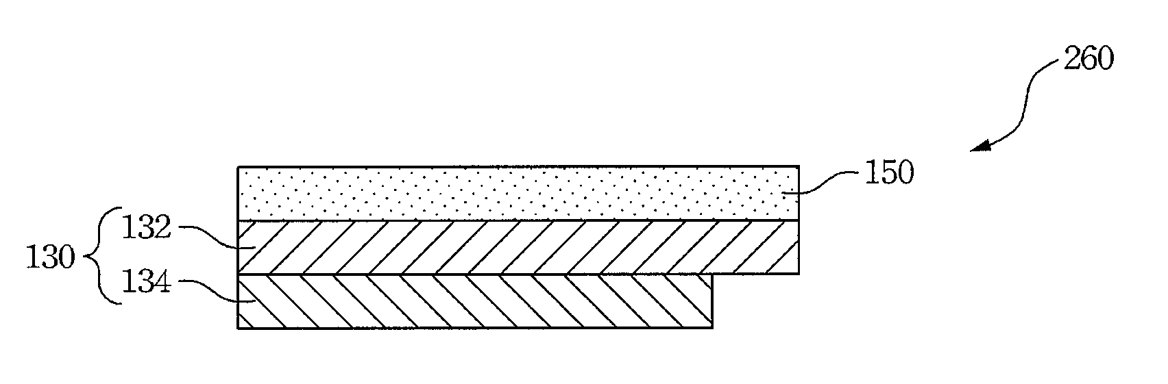
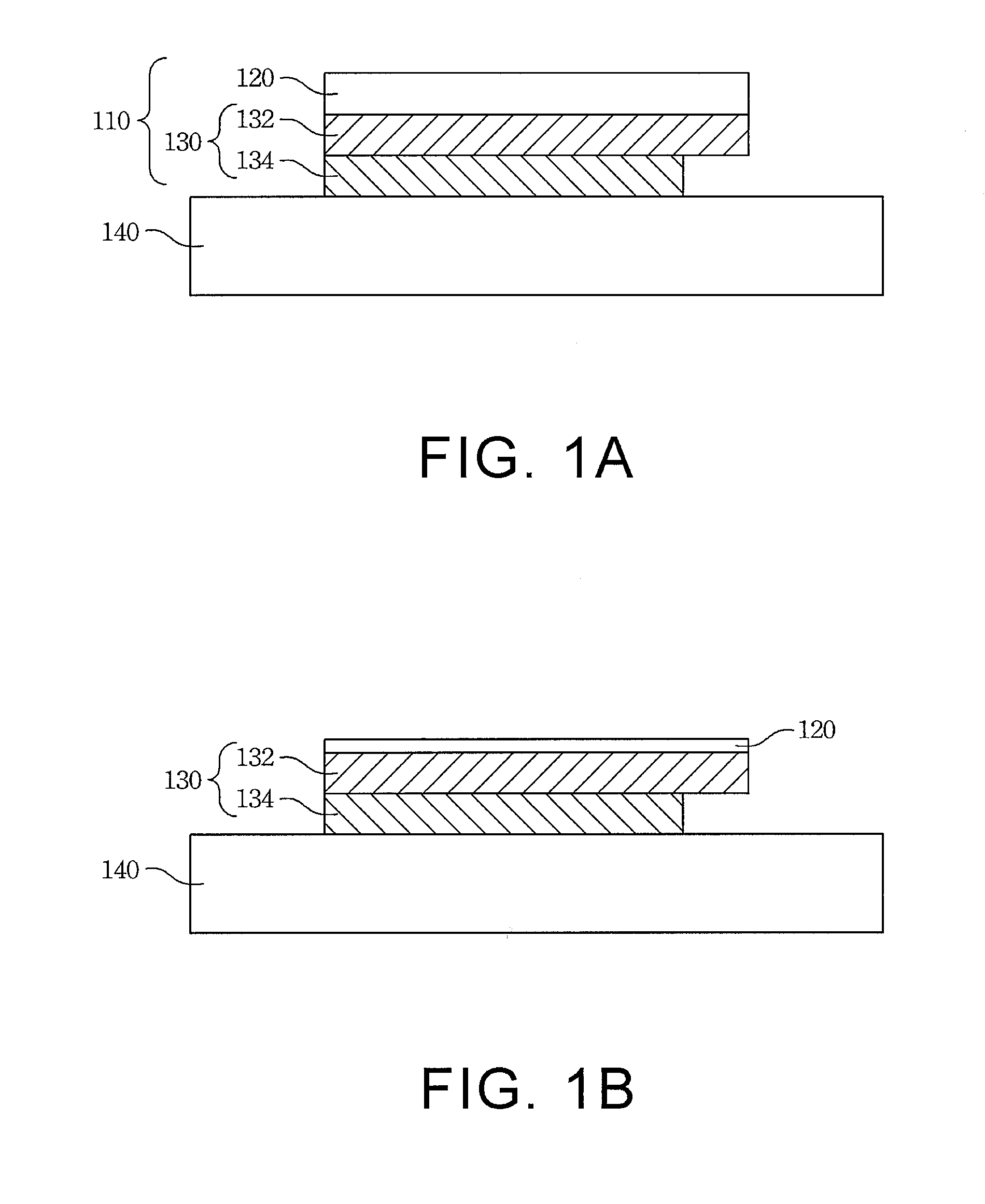
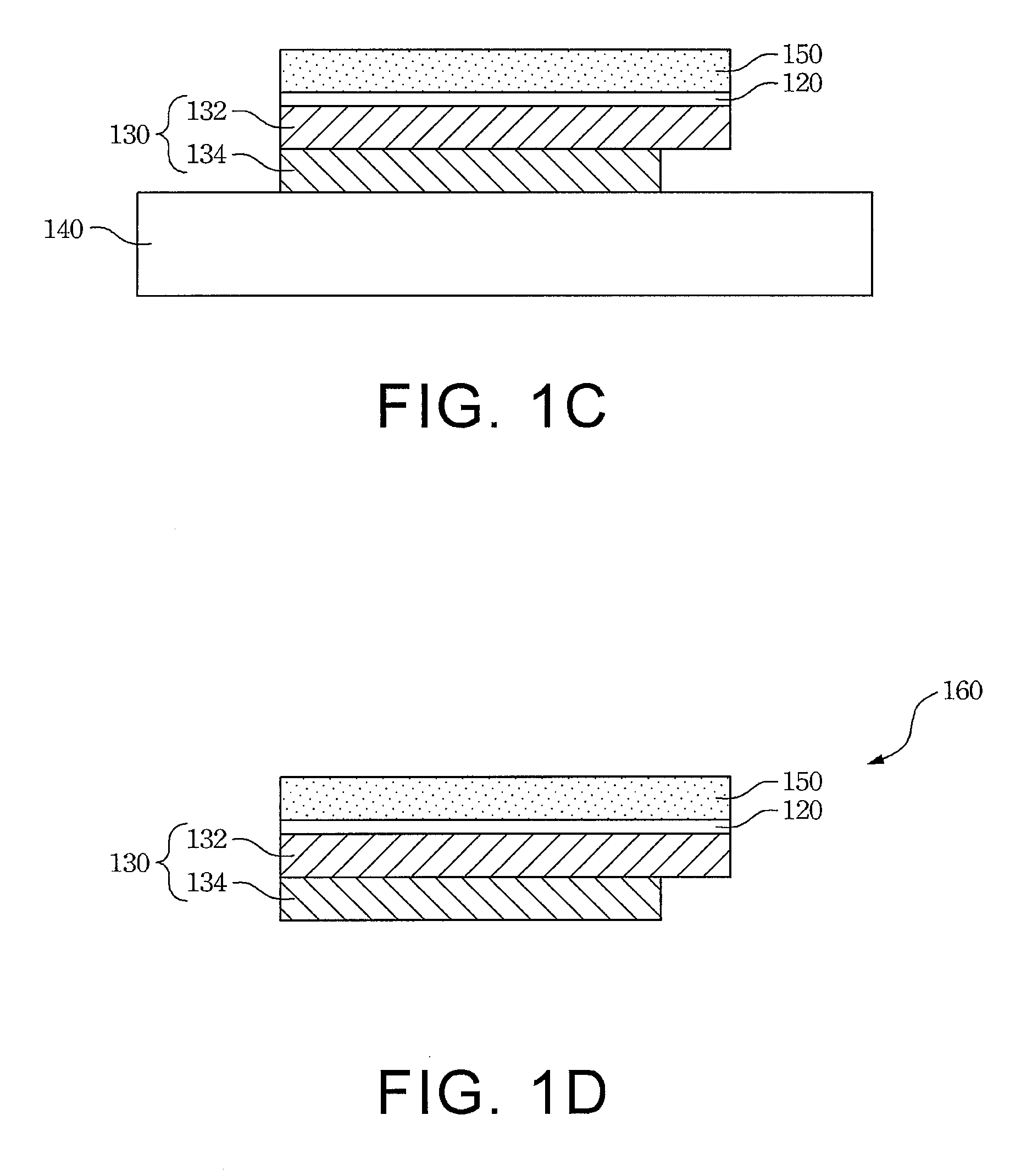
[0018]FIGS. 1A-1D are schematic cross-sectional flowcharts illustrating a manufacturing process of a light-emitting (LED) diode according to an embodiment of the present invention. In FIG. 1A, the semiconductor structure 110 is fixed on the supported base 140 as first, wherein the method for fixing can be, but not limited to, an adhesive bonding. The semiconductor structure 110 includes a sapphire substrate 120 and a semiconductor light-emitting layer 130, wherein a surface of the semiconductor light-emitting layer 130 covers and contacts with the sapphire substrate 120.
[0019]The aforementioned semiconductor light-emitting layer 130 at least includes a P-type semiconductor layer 132 and a N-type semiconductor layer 134, wherein the P-type semiconductor layer 132 and the N-type semiconductor layer 134 are stacked on the sapphire substrate 120. Herein, the position of the P-type semiconductor layer 132 and the N-type semiconductor layer 134 can be interchanged. The semiconductor light...
second embodiment
[0028]FIGS. 3A-3C are schematic cross-sectional flowcharts illustrating a manufacturing process of a light-emitting (LED) diode according to another embodiment of the present invention. Referring to FIG. 3A, a diamond film 350 is formed on the substrate 320 at first. The substrate 320 can be, for example, silicon substrate, aluminum oxide substrate, silicon nitride substrate, sapphire substrate or silicon carbide substrate.
[0029]Thereafter, referring to FIG. 3B, the semiconductor light-emitting layer 330 is formed on the diamond film 350 to form a LED 360. The aforementioned semiconductor light-emitting layer 330 at least includes a P-type semiconductor layer 332 and a N-type semiconductor layer 334, wherein the P-type semiconductor layer 332 and the N-type semiconductor layer 334 are stacked on the sapphire substrate 350. Herein, the position of the P-type semiconductor layer 332 and the N-type semiconductor layer 334 can be interchanged.
[0030]The aforementioned semiconductor light...
PUM
 Abstract
Description
Claims
Application Information