Image Forming Device and Image Forming Method

a technology of image forming and forming method, which is applied in the direction of electrographic process, recording apparatus, instruments, etc., can solve the problem of inability to achieve preferable latent image formation, and achieve the effect of simplifying the emission timing control of light emitting elements, preventing the influence of eccentricity, and high accuracy

Inactive Publication Date: 2011-05-26
SEIKO EPSON CORP
View PDF5 Cites 4 Cited by
  • Summary
  • Abstract
  • Description
  • Claims
  • Application Information

AI Technical Summary

Benefits of technology

[0006]In view of the problem described above, the invention has an advantage of providing a technology capable of preventing the misalignment of the position at which the latent image is formed caused by the variation in the moving velocity of the surface of the latent image carrier from occurring, thereby achieving preferable latent image formation.

Problems solved by technology

However, in the line head having a plurality of light emitting element groups disposed at positions different from each other in the width direction as described above, if a moving velocity of the surface of the latent image carrier varies, the position at which the latent image is formed is shifted in the sub-scanning direction, and in some cases, preferable latent image formation is not achievable.

Method used


Image

  • Image Forming Device and Image Forming Method
  • Image Forming Device and Image Forming Method
  • Image Forming Device and Image Forming Method

Examples


first embodiment

B. First Embodiment

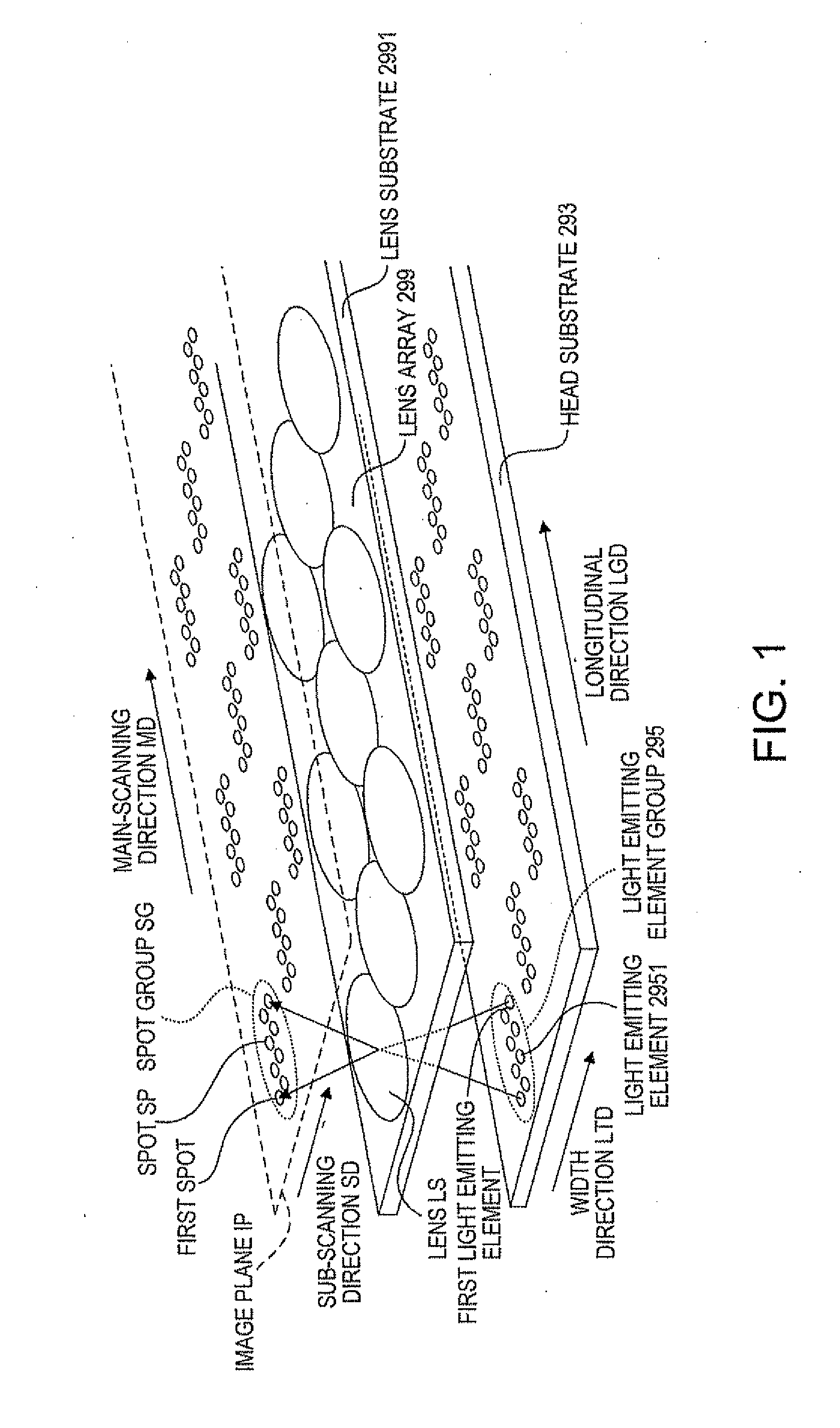
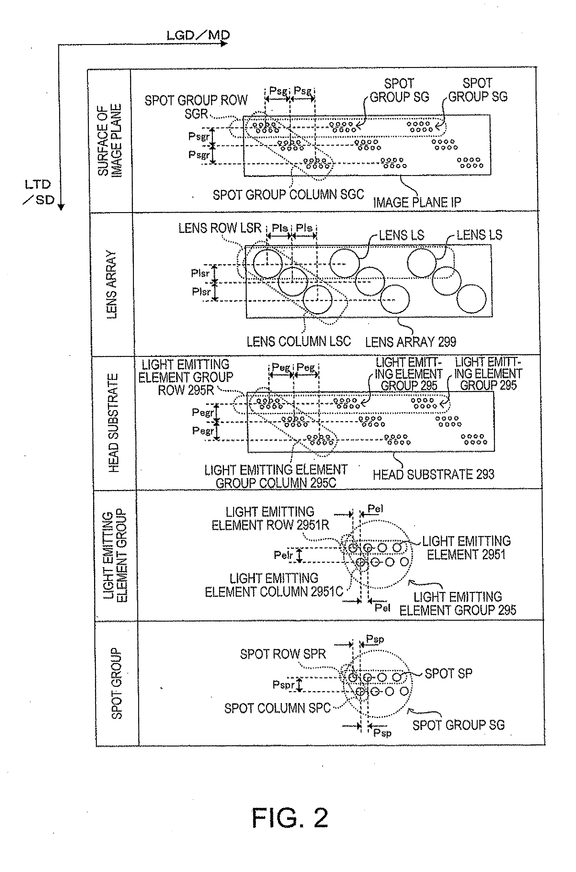
[0072]FIG. 3 is a diagram showing an example of an image forming device to which the invention can be applied. Further, FIG. 4 is a diagram showing an electrical configuration of the image forming device shown in FIG. 3. The device is an image forming device capable of selectively performing a color mode in which a color image is formed by overlapping four colors of toners of black (K), cyan (C), magenta (M), and yellow (Y), and a monochrome mode in which a monochrome image is formed using only the black (K) toner. It should be noted that FIG. 3 is a drawing corresponding to a state when performing the color mode. In the present image forming device, when an image formation command is provided to a main controller MC having a CPU, a memory, and so on from an external device such as a host computer, the main controller MC provides an engine controller EC with a control signal and so on, and a head controller HC with the video data VD corresponding to the image form...

second embodiment

C. Second Embodiment

[0125]In the first embodiment described above, the sub-scanning spot group pitch Psgs is set to be a value obtained by multiplying the sub-scanning pixel pitch Rsd by an integral number, and each of the light emitting element group rows 295R emits light at the same emission timing Tu. However, it is also possible to set the sub-scanning spot group pitch Psgs to be a value obtained by multiplying the sub-scanning pixel pitch Rsd by a non-integral number. On this occasion, the light emitting element group rows 295R_A, 295R_B, and 295R_C are provided with emission timings Tu_A, Tu_B, and Tu_C, respectively. Such a case will hereinafter be explained.

[0126]FIG. 21 is a block diagram showing a configuration of a head control block and so on in the second embodiment. Hereinafter, different points form the first embodiment will mainly be explained, and the common parts will be denoted with the corresponding reference marks, and the explanations therefor will be omitted. ...

third embodiment

D. Third Embodiment

[0133]Incidentally, in the first and second embodiments described above, the communication of the video data VD between the main controller MC and the head controller HC is executed with asynchronous serial communication. However, the communication method of the video data VD is not limited thereto.

[0134]FIG. 23 is a diagram showing a configuration of the main controller, the head controller, and the line head in a third embodiment. In the third embodiment, the head controller HC outputs the horizontal sync signal Hsync to the main controller MC for the video data VD. Meanwhile, the main controller MC outputs the video data VD to the head controller HC in sync with the horizontal sync signal Hsync. Further, the head controller HC, which has received the video data VD, discriminate the video data VD_A (for the light emitting element group row 295R_A), the video data VD_B (for the light emitting element group row 295R_B), and the video data VD_C (for the light emitt...


PUM


Abstract

An image forming device includes: an exposure head having a plurality of light emitting elements arranged in a first direction, a first imaging optical system adapted to image light emitted from the light emitting elements, and a second imaging optical system disposed in a second direction with respect to the first imaging optical system; a latent image carrier movable in the second direction; a detection section adapted to detect a moving time the latent image carrier takes to move from a first position to a second position in the second direction; and a control section adapted to control the time from emission of a first part of the light emitting elements adapted to emit light to be imaged by the first imaging optical system to emission of a second part of the light emitting elements adapted to emit light to be imaged by the second imaging optical system based on the detection result of the detection section, thereby aligning a latent image formed on the latent image carrier by the first imaging optical system and a latent image formed on the latent image carrier by the second imaging optical system in the first direction.

Description

BACKGROUND[0001]1. Technical Field[0002]The present invention relates to an image forming device and an image forming method using an exposure head adapted to image a light beam emitted from a light emitting element with an imaging optical system.[0003]2. Related Art[0004]As the exposure head of this kind, there is known a line head adapted to image light beams emitted from a plurality of light emitting elements as a plurality of spots. In the line head (the exposure head in the document) described in JP-A-2004-66758, for example, there are arranged a corresponding number of light emitting elements to one line in a direction corresponding to the main scanning direction, and the light beams emitted from the respective light emitting elements are imaged as spots by a gradient index lens. Then, by sequentially forming a latent image of every line on a surface of a latent image carrier moving in a sub-scanning direction, a two-dimensional latent image corresponding to a desired image ca...

Claims


Application Information

Patent Timeline
Patent Type & Authority Applications(United States)
IPC IPC(8): G03G15/043
CPCB41J2/451
Inventor NOMURA, YUJIROINOUE, NOZOMUTSUJINO, KIYOSHIKOIZUMI, RYUTA
Owner SEIKO EPSON CORP
Why Eureka
Try Eureka