PHOTOCONDUCTOR DEVICE HAVING POLYCRYSTALLINE GaAs THIN FILM AND METHOD OF MANUFACTURING THE SAME

a technology of photoconductor and thin film, which is applied in the field of photoconductor devices, can solve the problems of low reliability, reduce productivity, increase price, etc., and achieve the effects of low reliability, reduced productivity, and precise process

Inactive Publication Date: 2011-06-02
ELECTRONICS & TELECOMM RES INST
View PDF8 Cites 18 Cited by
  • Summary
  • Abstract
  • Description
  • Claims
  • Application Information

AI Technical Summary

Benefits of technology

[0015]The present invention is directed to a photoconductor device having a polycrystalline GaAs thin film and a method of manufacturing the same in which the above-mentioned problems of a single crystalline material used in the photoconductor are solved. In order to obtain an existing single crystalline material, high-price equipment called a molecular beam epitaxy system has to be used, and the crystal defect has to be controlled through a very precise process. Further, long-term use changes a defect distribution and a characteristic, leading to low reliability. This reduces productivity and increases the price in the case of commercialization. Further, in the case of actual use, in order to obtain spectrum information, it is necessary to obtain a reference spectrum of the terahertz (THz) wave itself. However, since the status of the photoconductor and device varies from time to time depending on ambient temperature, an electrical characteristic, and the frequency of practical use, it is necessary to continuously measure and detect for actual stable application. Therefore, the method most commonly used now employs the single crystalline material, but in order to prepare for future mass demand, reliability, reproducibility, and economical efficiency of a material have to be secured.

Problems solved by technology

Further, long-term use changes a defect distribution and a characteristic, leading to low reliability.
This reduces productivity and increases the price in the case of commercialization.

Method used


Image

  • PHOTOCONDUCTOR DEVICE HAVING POLYCRYSTALLINE GaAs THIN FILM AND METHOD OF MANUFACTURING THE SAME
  • PHOTOCONDUCTOR DEVICE HAVING POLYCRYSTALLINE GaAs THIN FILM AND METHOD OF MANUFACTURING THE SAME
  • PHOTOCONDUCTOR DEVICE HAVING POLYCRYSTALLINE GaAs THIN FILM AND METHOD OF MANUFACTURING THE SAME

Examples


Embodiment Construction

[0032]Hereinafter, exemplary embodiments of the present invention will be described in detail. However, the present invention is not limited to the embodiments disclosed below, but can be implemented in various forms. The following embodiments are described in order for this disclosure to be complete and enabling to those of ordinary skill in the art.

[0033]When an element is referred to as being “on” or “below” another element, it can be directly on or directly below the other element or layer, or intervening elements may be present. In the drawings, the size and relative sizes of layers and regions may be exaggerated for clarity.

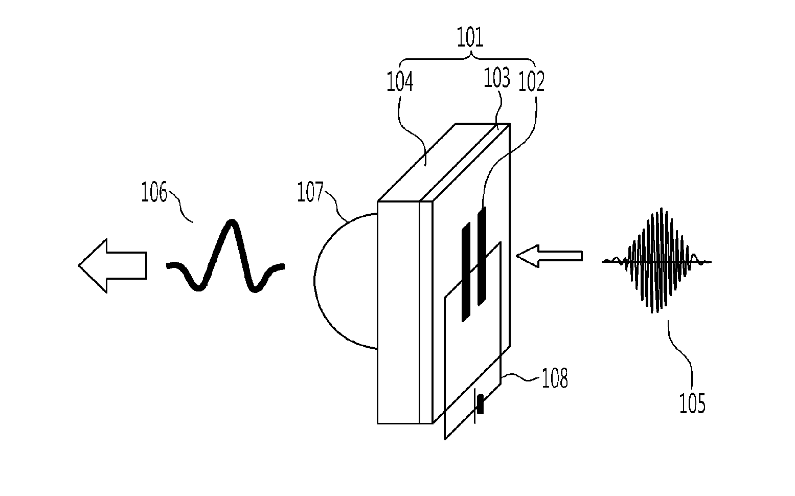
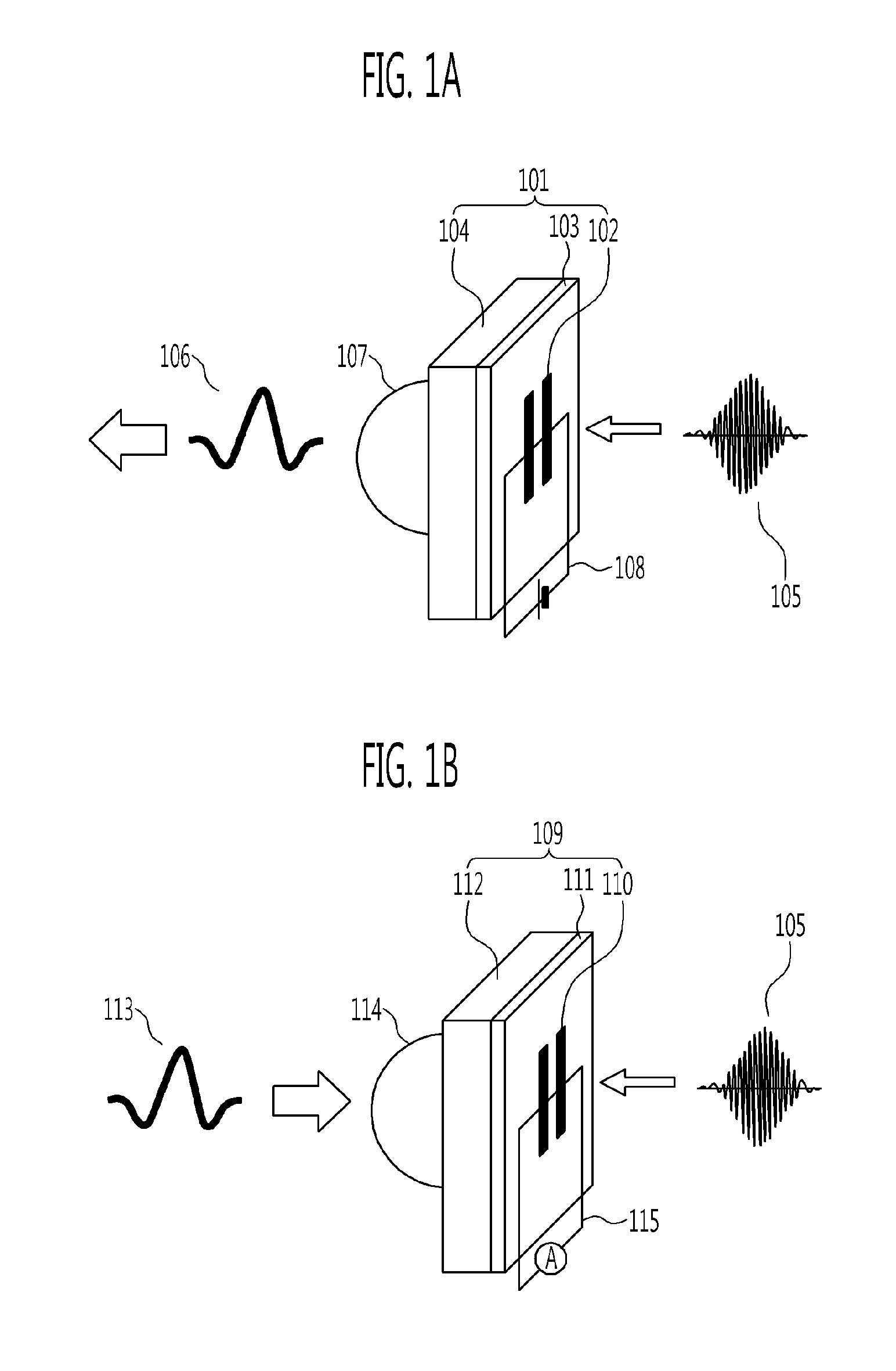
[0034]A photoconductive antenna device using a polycrystalline GaAs thin film according to an exemplary embodiment of the present invention will be described below with reference to FIGS. 1A and 1B.

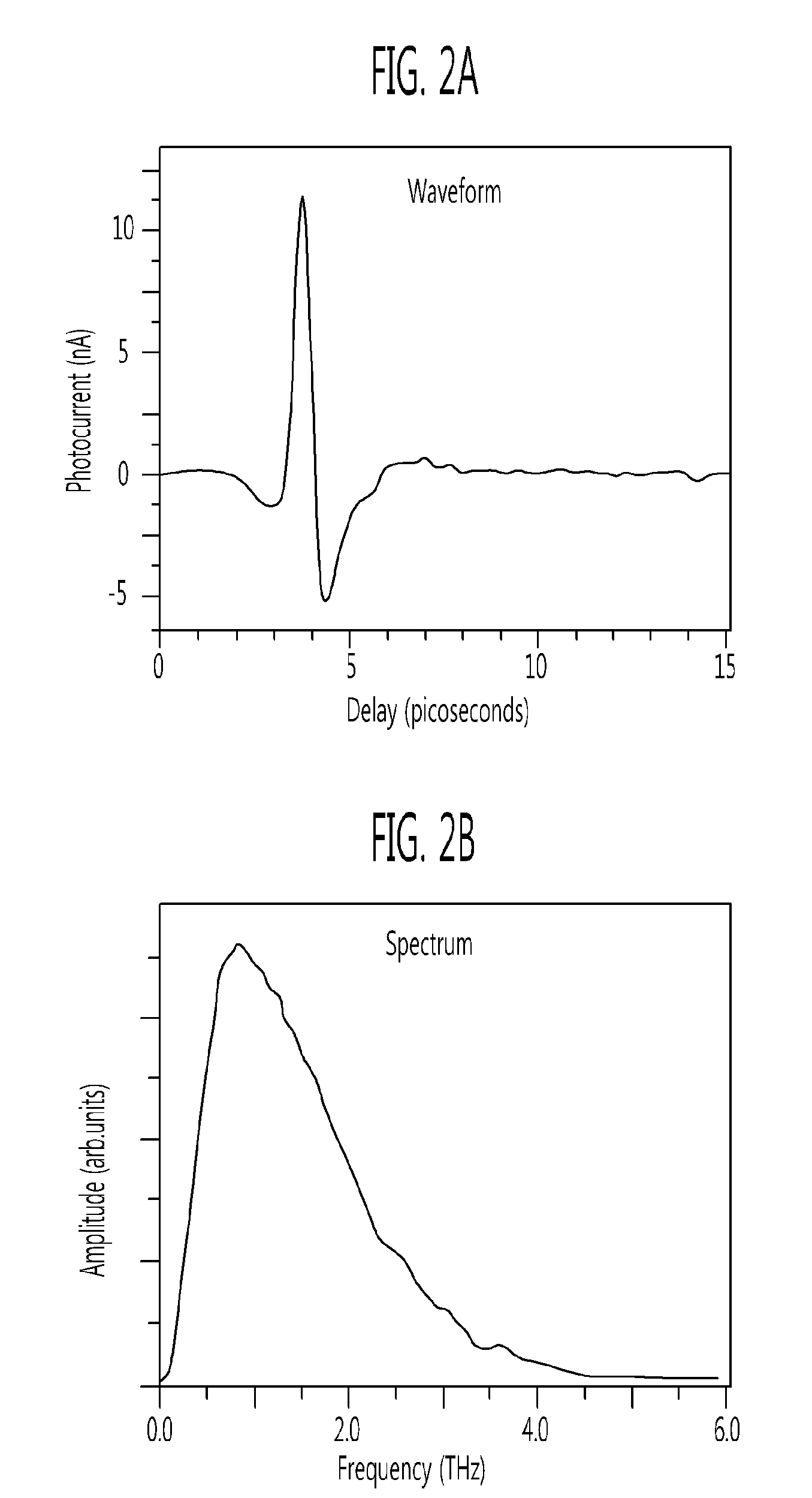
[0035]FIGS. 1A and 1B illustrate the configuration of a photoconductive antenna using a polycrystalline GaAs thin film as a device for generating and detecting t...


PUM

PropertyMeasurementUnit
absolute temperatureaaaaaaaaaa
bias voltageaaaaaaaaaa
distanceaaaaaaaaaa

Abstract

A photoconductor device and a method of manufacturing the same are provided. The photoconductor device includes a photoconductor substrate, a photoconductor thin film deposited on the photoconductor substrate, and a photoconductive antenna electrode formed on the photoconductor thin film. The photoconductor thin film includes polycrystalline GaAs.

Description

CROSS-REFERENCE TO RELATED APPLICATION[0001]This application claims priority to and the benefit of Korean Patent Application No. 10-2009-0118339, filed Dec. 2, 2009, the disclosure of which is incorporated herein by reference in its entirety.BACKGROUND[0002]1. Field of the Invention[0003]The present invention relates to a photoconductor device which generates or detects a terahertz (THz) wave, and more particularly, to a material for a photoconductor device.[0004]2. Discussion of Related Art[0005]A terahertz (THz) wave is an electromagnetic wave which corresponds to a frequency domain between 0.1 THz to 10 THz and is an intermediate wave between a radio wave and a light wave. The THz wave has a shorter wavelength than a radio wave with the shortest wavelength, a millimeter wave, and a longer wavelength than a light wave with the longest wavelength, a far infrared ray. One (1) THz is a value which corresponds to a wavelength of 30 μm, a wave number of 33.3 cm−1, a time of one pico (1...

Claims


Application Information

Patent Timeline
Patent Type & Authority Applications(United States)
IPC IPC(8): H01L31/0304H01L31/18H01L31/09H01L31/0232H01L33/58H01L33/02
CPCG01J3/42A61B1/07G01R29/14H01L31/101
Inventor PAEK, MUN CHEOL
Owner ELECTRONICS & TELECOMM RES INST
Why Eureka
Try Eureka