Lateral super junction device with high substrate-drain breakdwon and built-in avalanche clamp diode

Active Publication Date: 2011-06-02
ALPHA & OMEGA SEMICON INC
View PDF6 Cites 43 Cited by
  • Summary
  • Abstract
  • Description
  • Claims
  • Application Information

AI Technical Summary

Benefits of technology

[0007]It is therefore an aspect of the present invention to provide a new and improved device structure and manufacturing method to form the junction field effect transistor (JFET) power device on a P substrate with lateral super junction structure extended betwee

Problems solved by technology

However, the manufacturing technologies and device configuration for implementing the super-junction structures in the MOSFET devices are still confronted with manufacturability difficulties.
The manufacturing ease and cost of the conventional vertical high voltage power devices implemented with super-junction structures are limited due to the structural features that require numerous time-consuming, complex, and expensive manufacturing processes.
Achieving a high density of alternately doped columns becomes prohibitive since it requires a direct increase in the number of these steps.
It is difficult and costly to manufa

Method used


Image

  • Lateral super junction device with high substrate-drain breakdwon and built-in avalanche clamp diode
  • Lateral super junction device with high substrate-drain breakdwon and built-in avalanche clamp diode
  • Lateral super junction device with high substrate-drain breakdwon and built-in avalanche clamp diode

Examples


Embodiment Construction

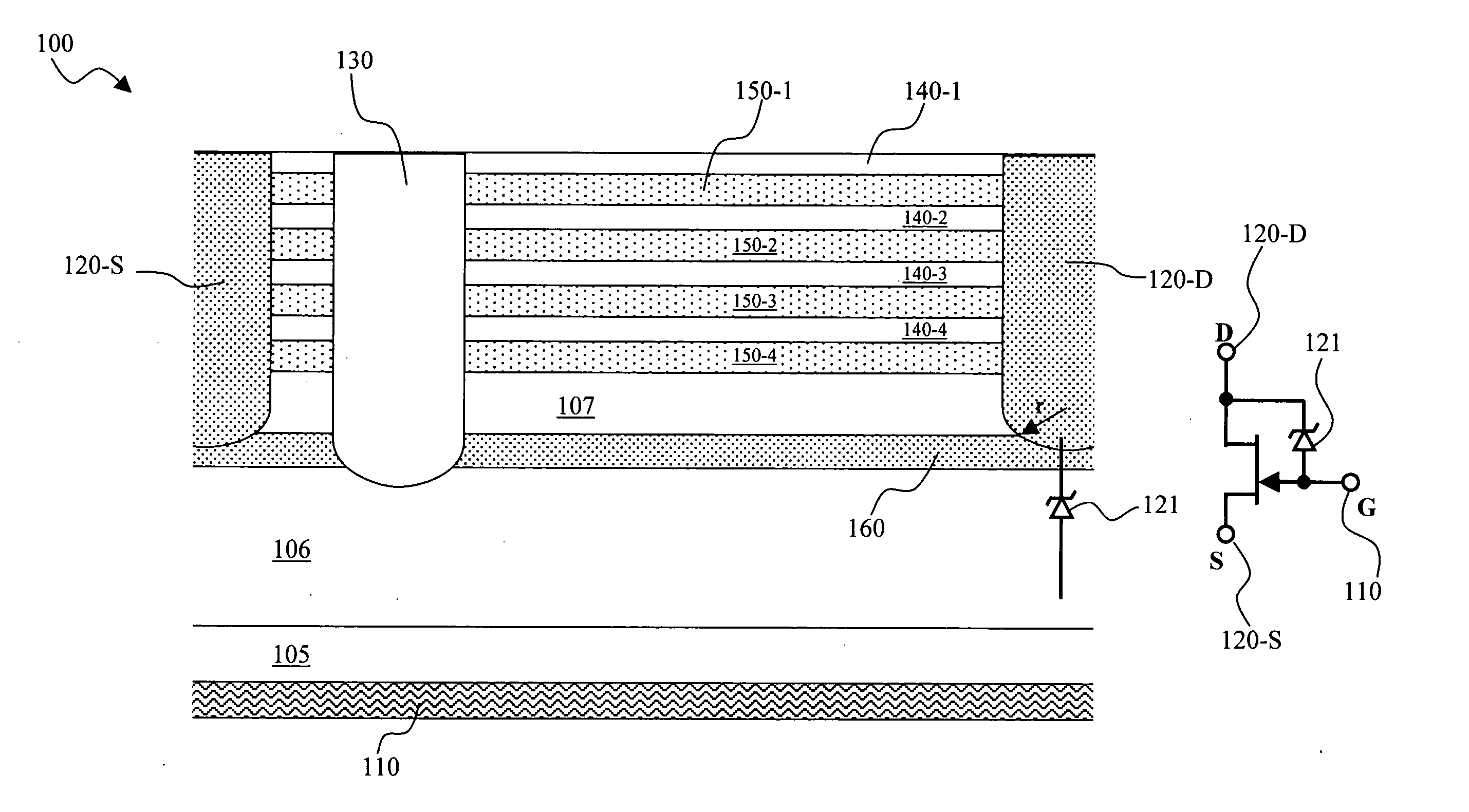
[0034]Referring to FIG. 2 for a cross sectional view of a lateral power device 100 that illustrates the new concepts including the new structural and manufacturing features of this invention. The lateral power device 100 is supported on a P+ substrate 105 that includes a gate metal electrode 110 disposed on the bottom of the substrate. The P+ substrate 105 may further comprise a P Epi layer 106 on top of it. The lateral power device 100 includes a source and a drain formed as N+ column 120-S and N+ column 120-D, respectively, disposed in a first and second trench at two opposite sides of the semiconductor substrate. A P+ doped column 130 disposed in another trench functions as a gate of the lateral power device. The P+ doped column 130 connects to the P-Epi 106, thus the P+ substrate 105 is biased to the gate, and a gate metal 110 may be located at the bottom of P+ substrate 105 to control the gate column 130. The source and drain 120-S and 120-D may be formed with N+ doped polysili...


PUM


Abstract

This invention discloses configurations and methods to manufacture lateral power device including a super junction structure with an avalanche clamp diode formed between the drain and the gate. The lateral super-junction structure reduces on-resistance, while the structural enhancements, including an avalanche clamping diode and an N buffer region, increase the breakdown voltage between substrate and drain and improve unclamped inductive switching (UIS) performance.

Description

BACKGROUND OF THE INVENTION[0001]1. Field of the Invention[0002]The invention relates generally to semiconductor power devices. More particularly, this invention relates to configurations and methods to manufacture lateral power device including a super-junction structure with an avalanche clamp diode formed between the drain and the gate. The lateral super-junction structure reduces on-resistance, while the structural enhancements increase the breakdown voltage between substrate and drain and improve unclamped inductive switching (UIS) performance.[0003]2. Description of the Prior Art[0004]Conventional semiconductor power device such as the MOSFET power devices implemented with a super-junction structure can achieve performance improvements with significant reduction of the on-resistance while still maintaining a high breakdown voltage. However, the manufacturing technologies and device configuration for implementing the super-junction structures in the MOSFET devices are still con...

Claims


Application Information

Patent Timeline
IPC IPC(8): H01L27/06H01L21/8234
CPCH01L27/0705H01L29/808H01L29/66901H01L29/0634H01L2224/48091H01L2224/48247H01L2924/181H01L2224/0603H01L2224/48257H01L2924/13091H01L2924/00014H01L2924/00012H01L2924/00
Inventor BOBDE, MADHURBHALLA, ANUPYILMAZ, HAMZAMA, WILSONGUAN, LINGPENGLEE, YEEHENGCHEN, JOHN
Owner ALPHA & OMEGA SEMICON INC
Why Eureka
Try Eureka