Connection structure of electronic component and wired circuit board, wired circuit board assembly, and method for testing electronic component

a technology of wired circuit board and electronic component, which is applied in the direction of functional testing of recording heads, instruments, and recording information storage, etc., can solve the problems of reduced connection strength between patterning end portions of conductive layers and the terminals of magnetic heads, narrow spacing between terminals, etc., to reduce the volume of connection, excellent connection, and suppress swelling and bulging of solder

Inactive Publication Date: 2011-06-02
NITTO DENKO CORP
View PDF3 Cites 11 Cited by
  • Summary
  • Abstract
  • Description
  • Claims
  • Application Information

AI Technical Summary

Benefits of technology

[0031]In such a wired circuit board assembly, by the reaction force of the warping of the wired circuit board, the terminal portions and the external terminals are abutted, and therefore by reducing the solder volume for connection, swelling and bulging of the solder is suppressed, and at the same time, the electronic component and the wired circuit board are excellently connected.
[0032]Therefore, in such a wired circuit board assembly, even in the case of a high density hard disk drive and narrow terminal spacing, excellent connection reliability is ensured, and a short circuit between the terminal portions and the external terminals can be prevented.

Problems solved by technology

However, in a head slider designed for a high density hard disk drive, spacing between the terminals is narrow.
On the other hand, for example, when the volume of the solder ball is reduced to suppress the swelling and bulging of the solder ball, there is a disadvantage in that the connection strength between the patterning end portion of the conductive layer and the terminal of the magnetic head is reduced.
Also, with the method described in Japanese Unexamined Patent Publication No. 2007-128634, because it is usually difficult to completely re-melt and remove the solder, residual solder may be present at the terminal of the slider that was taken out from the test head suspension assembly (that is, the terminal is contaminated).

Method used


Image

  • Connection structure of electronic component and wired circuit board, wired circuit board assembly, and method for testing electronic component
  • Connection structure of electronic component and wired circuit board, wired circuit board assembly, and method for testing electronic component
  • Connection structure of electronic component and wired circuit board, wired circuit board assembly, and method for testing electronic component

Examples


Embodiment Construction

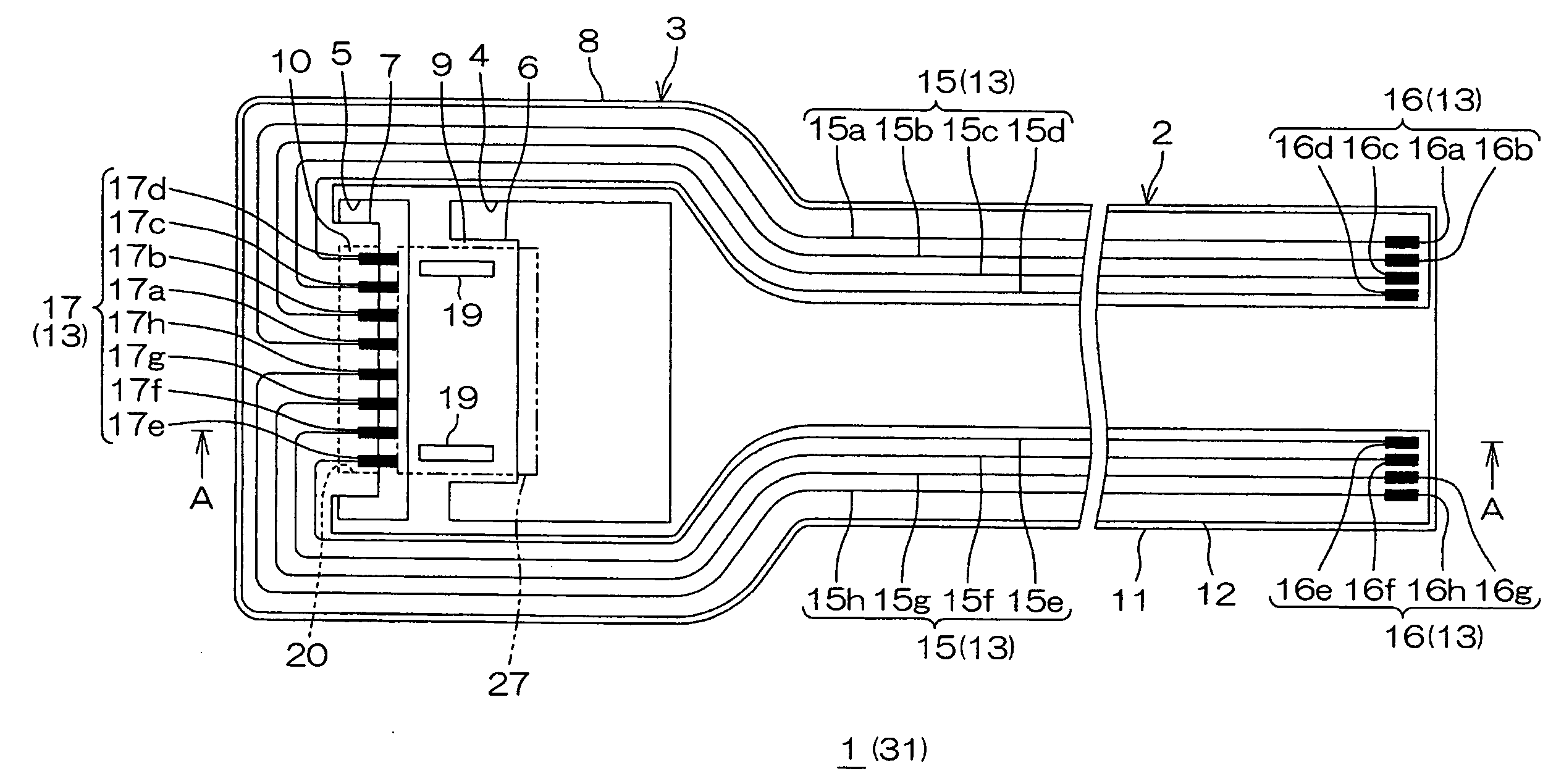
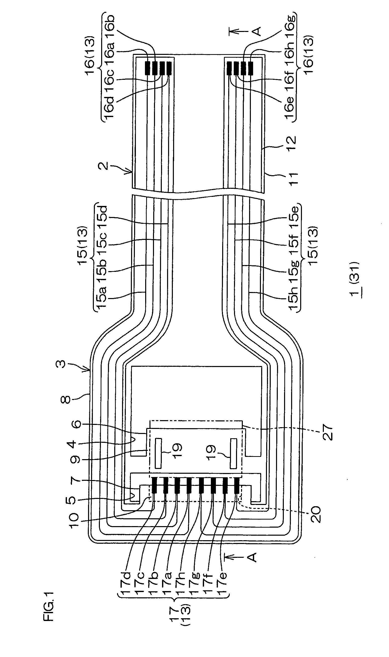
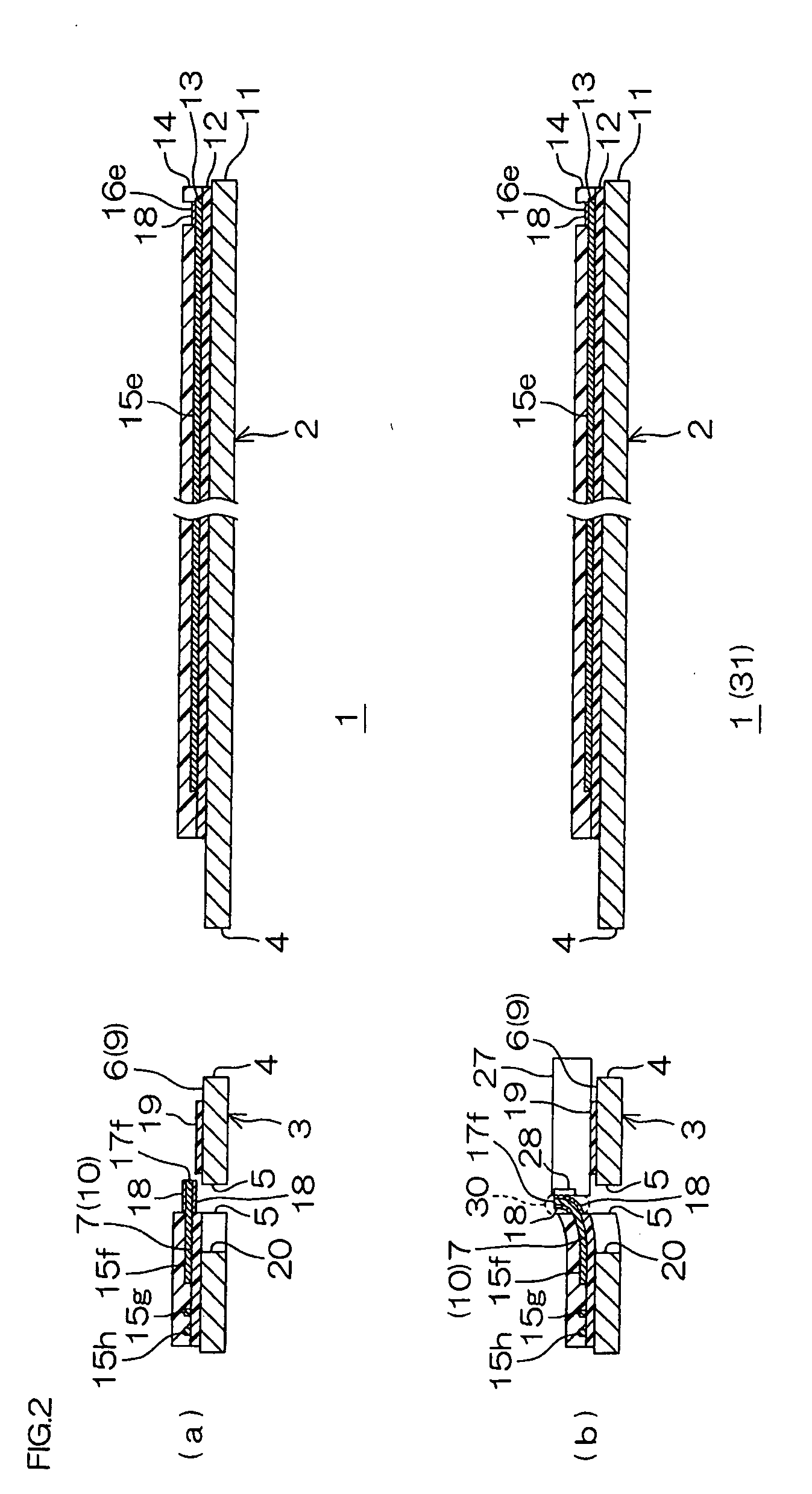
[0048]FIG. 1 shows a plan view of a suspension board with circuits that is used in a connection structure of a head slider and a suspension board with circuits as an embodiment of a connection structure of an electronic component and a wired circuit board of the present invention; FIG. 2 shows cross-sectional views illustrating a connection structure of a head slider and a suspension board with circuits as an embodiment of a connection structure of an electronic component and a wired circuit board of the present invention: (a) illustrating a cross-sectional view taken along line A-A of the suspension board with circuits shown in FIG. 1 before connecting a head slider; and (b) illustrating a cross-sectional view taken along line A-A of the suspension board with circuits shown in FIG. 1 after connecting a head slider. In FIG. 1, an insulating cover layer 14 (described later) is omitted to clearly show the relative position of the conductive pattern 13.

[0049]In FIG. 1, on a suspension ...


PUM

PropertyMeasurementUnit
thicknessaaaaaaaaaa
thicknessaaaaaaaaaa
thicknessaaaaaaaaaa

Abstract

In a connection structure of an electronic component and a wired circuit board, the electronic component includes a plurality of external terminals. The wired circuit board includes a metal supporting board, an insulating base layer formed on the metal supporting board, and a conductive pattern formed on the insulating base layer. The conductive pattern includes a plurality of terminal portions for connection with the plurality of external terminals. The electronic component and the wired circuit board are disposed such that the plurality of external terminals and the plurality of terminal portions face each other. The wired circuit board is bent such that the conductive pattern is warped, and by the reaction force of the warping, the terminal portions and the external terminals are abutted, and the electronic component and the wired circuit board are electrically connected.

Description

CROSS-REFERENCE TO RELATED APPLICATION[0001]The present application claims priority from U.S. Provisional Patent Application No. 61 / 282,060 filed on Dec. 9, 2009, and from Japanese Patent Application No. 2009-273693 filed on Dec. 1, 2009, the contents of which are hereby incorporated by reference into this application.BACKGROUND OF THE INVENTION[0002]1. Field of the Invention[0003]The present invention relates to a connection structure of an electronic component and a wired circuit board, a wired circuit board assembly, and a method for testing an electronic component. To be specific, the present invention relates to a connection structure of an electronic component such as a head slider and a wired circuit board such as a suspension board with circuits; a wired circuit board assembly including the connected electronic component and wired circuit board; and a method for testing an electronic component.[0004]2. Description of the Related Art[0005]Conventionally, in magnetic recording...

Claims


Application Information

Patent Timeline
Patent Type & Authority Applications(United States)
IPC IPC(8): G01R31/304H05K1/00H05K3/30
CPCG11B5/486H05K1/118H05K1/056H05K3/4092H05K2201/091H05K3/326Y10T29/4913H05K3/305G11B5/455
Inventor OHSAWA, TETSUYAKANAGAWA, HITOKI
Owner NITTO DENKO CORP
Why Eureka
Try Eureka