Impedance adjusting device

a technology of impedance adjusting and adjusting device, which is applied in the direction of logic circuit coupling/interface arrangement, pulse technique, instruments, etc., can solve the problems of increasing the influence of external noise, and increasing the reflectivity of signal reflectivity due to impedance mismatching at interfaced terminals. , to achieve the effect of increasing the accuracy of calibration and termination operations, and not increasing the number of impedance code bits

Inactive Publication Date: 2011-06-02
SK HYNIX INC
View PDF5 Cites 44 Cited by
  • Summary
  • Abstract
  • Description
  • Claims
  • Application Information

AI Technical Summary

Benefits of technology

[0024]An embodiment of the present invention is directed to an impedance adjusting device which is capable of increasing the accuracy of the calibration and termination operations, without increasing the number of impedance code bits.

Problems solved by technology

However, as the amplitude swings of the signals are reduced, the influence of external noise is increased, and signal reflectivity due to impedance mismatching at interfaced terminals becomes more severe.
The impedance mismatching is caused by external noise or variations in power supply voltage, operating temperature or fabrication process.
When impedance mismatching occurs, high-speed data transmission may be difficult, and data outputted from data output terminals of the semiconductor device may be distorted.
Therefore, when the receiving circuit of the semiconductor device receives the distorted output signals through the input terminals, setup / hold failure or an incorrect determination of input levels may frequently occur.
However, if the number of bits of the impedance codes PCODE and NCODE is increased, then the complexity of the calibration circuit is also increased.

Method used


Image

  • Impedance adjusting device
  • Impedance adjusting device
  • Impedance adjusting device

Examples


Embodiment Construction

[0039]Exemplary embodiments of the present invention are described below in detail with reference to the accompanying drawings. The present invention may, however, be embodied in different forms and should not be constructed as being limited to the embodiments set forth herein. Rather, these embodiments are provided so that this disclosure will be thorough and complete, and will fully convey the scope of the present invention to those skilled in the art. Throughout the disclosure, like reference numerals refer to like parts throughout the various figures and embodiments of the present invention.

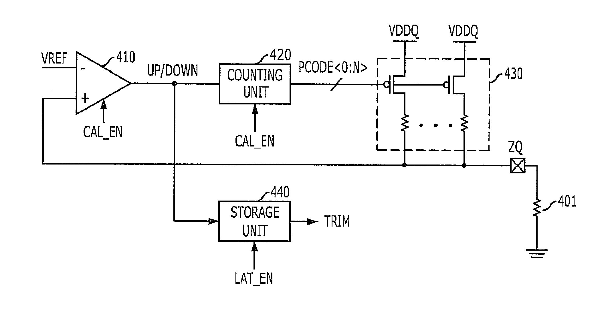
[0040]An impedance adjusting device includes a calibration circuit and a termination circuit.

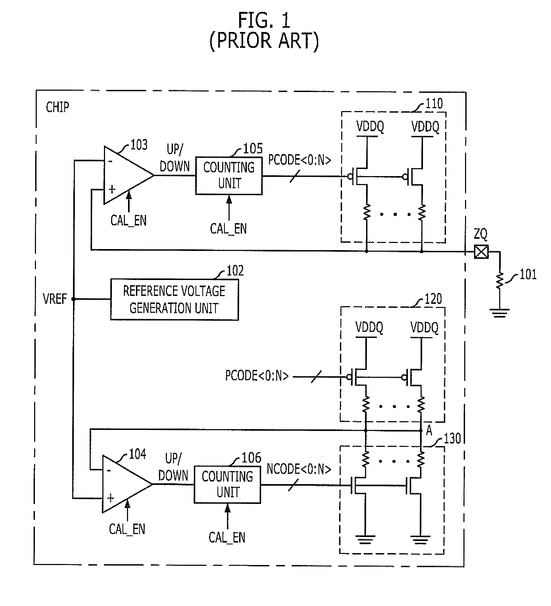
[0041]FIG. 4 is a diagram of a calibration circuit of an impedance adjusting device according to a first embodiment of the present invention. In the first embodiment of the present invention, the calibration circuit (see FIG. 4) generates a single impedance code, and the termination circuit (see FIG. ...


PUM


Abstract

An impedance adjusting device includes: a calibration node; a comparison unit configured to compare a reference voltage with a voltage of the calibration node; a counting unit configured to generate an impedance code according to a comparison result of the comparison unit; a reference impedance unit having an impedance value according to the impedance code and connected to the calibration node; a storage unit configured to store the comparison result of the comparison unit upon the generation of the impedance code being completed; an interface node; and a termination unit configured to terminate the interface node, the termination unit including a plurality of parallel resistors configured to be turned on / off according to the impedance code, and a parallel resistor configured to be turned on / off according to a value stored in the storage unit.

Description

CROSS-REFERENCE TO RELATED APPLICATIONS[0001]The present application claims priority of Korean Patent Application No. 10-2009-0117428, filed on Nov. 30, 2009, which is incorporated herein by reference in its entirety.BACKGROUND OF THE INVENTION[0002]An embodiment of the present invention relates to an impedance adjusting device for matching impedances of input / output pads for communication with external circuits in a semiconductor device.[0003]A variety of semiconductor devices are implemented with integrated circuit chips, such as CPUs, memories, and gate arrays. Such semiconductor devices are incorporated in various electronic products, such as personal computers, servers, and workstations. In most cases, semiconductor devices include receiving circuits to receive a variety of external signals through input pads, and output circuits to output a variety of internal signals through output pads.[0004]Meanwhile, as the operating speeds of the electronic products increase, amplitude sw...

Claims


Application Information

Patent Timeline
Patent Type & Authority Applications(United States)
IPC IPC(8): H03K19/003
CPCG11C7/02G11C7/04G11C7/1051G11C7/1057G11C2207/2254G11C29/025G11C29/028G11C29/50008G11C29/02G11C7/1048H03K19/017545H04L25/0278G11C2207/105
Inventor KO, HYEONG-JUN
Owner SK HYNIX INC
Why Eureka
Try Eureka