

Solid-state image pickup device, method of manufacturing the same, and electronic apparatus
- Summary
- Abstract
- Description
- Claims
- Application Information
AI Technical Summary
Benefits of technology
Problems solved by technology
Method used
Image

Examples
second embodiment
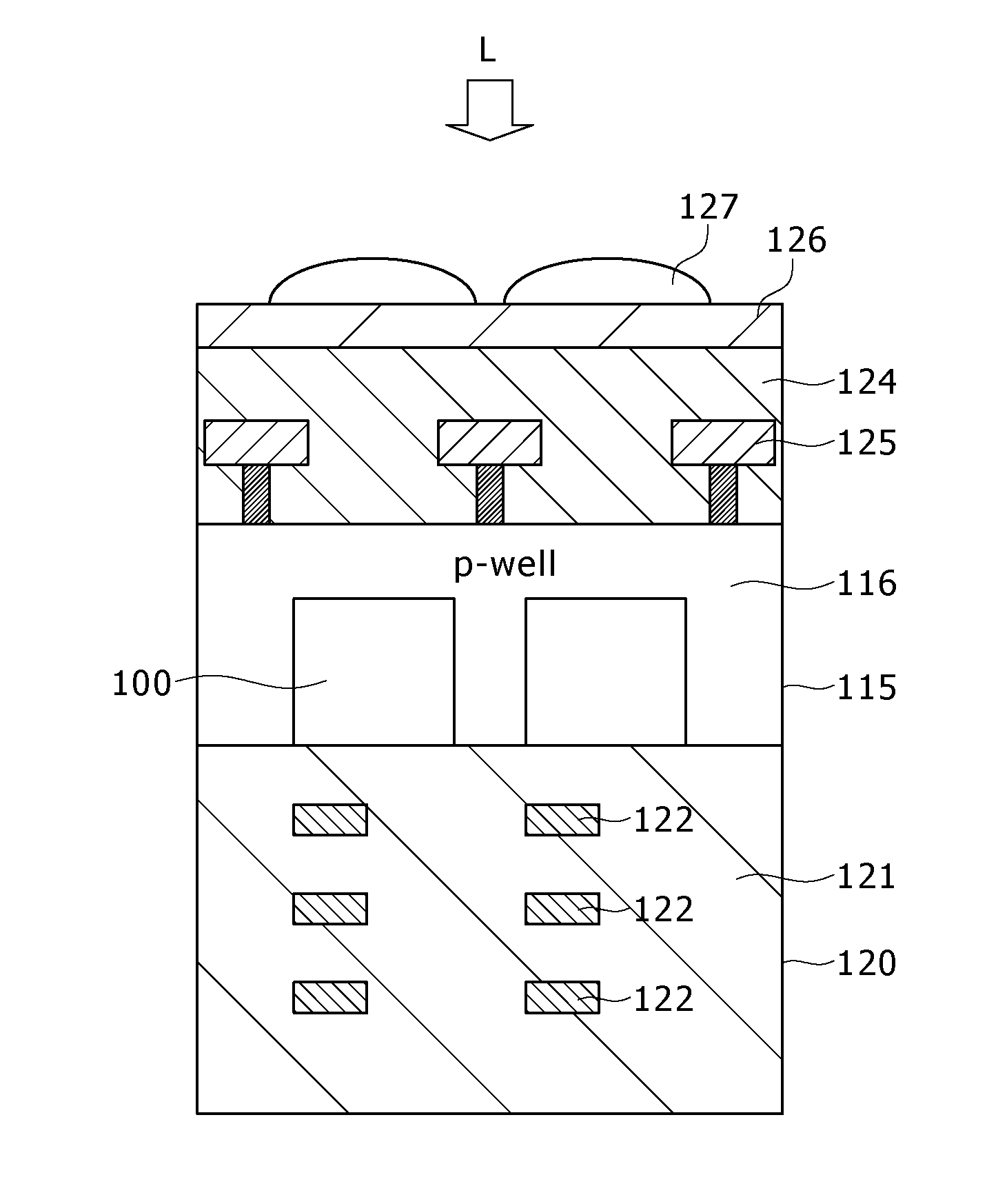
2. Solid-State Image Pickup Device
Next, a solid-state image pickup device according to the second embodiment of the present invention will be described with reference to FIG. 12. Although in the solid-state image pickup device 1 of the first embodiment, the light blocking film 23 serves as the wiring as well for the substrate potential, in the solid-state image pickup device 1 of the second embodiment, the light blocking film 23 and the wiring for the substrate potential are formed independently of each other.
FIG. 12 is a cross sectional view showing a schematic structure of the solid-state image pickup device according to the second embodiment of the present invention. In FIG. 12, portions corresponding to those in FIG. 4A are designated by the reference numerals, respectively, and a repeated description thereof is omitted here for the sake of simplicity. In the solid-state image pickup device 1 of the second embodiment, a wiring 55 for a substrate potential which serves to fix th...
third embodiment
3. Solid-State Image Pickup Device
Next, a solid-state image pickup device according to a third embodiment of the present invention will be described with reference to FIGS. 15A and 15B. The solid-state image pickup device of the third embodiment is different in the section for applying the potential to the wiring for the substrate potential from the solid-state image pickup device of the first embodiment.
FIG. 15A is a cross sectional view showing a schematic structure of the solid-state image pickup device according to the third embodiment of the present invention. Also, FIG. 15B is a top plan view showing a structure of a main portion of the solid-state image pickup device shown in FIG. 15A. In FIG. 15A, portions corresponding to those in FIG. 4A are designated by the same reference numerals, respectively, and a repeated description thereof is omitted here for the sake of simplicity.
In the third embodiment, as shown in FIG. 15A, a front surface side contact portion 60 through whic...
fourth embodiment
4. Electronic Apparatus
Next, an electronic apparatus according to a fourth embodiment of the present invention will be described with reference to FIG. 16. FIG. 16 is a block diagram showing a schematic configuration of an electronic apparatus 200 according to the fourth embodiment of the present invention.
The electronic apparatus 200 of the fourth embodiment corresponds to the case where the image pickup device 1 according to the first embodiment of the present invention described above is used in the electronic apparatus (camera).
The electronic apparatus 200 of the fourth embodiment has the image pickup device 1, an optical lens 210, a shutter arrangement 211, a driving circuit 212, and a signal processing circuit 213.
The optical lens 210 forms an image light (incident light) from a subject as an image on an imaging area of the image pickup device 1. As a result, the signal electric charges concerned are accumulated in the image pickup device 1 for a given period of time.
The shut...
PUM
 Abstract
Description
Claims
Application Information