CMOS image sensor capable of performing analog correlated double sampling

Active Publication Date: 2006-10-05
INTELLECTUAL VENTURES II
View PDF1 Cites 11 Cited by
  • Summary
  • Abstract
  • Description
  • Claims
  • Application Information

AI Technical Summary

Benefits of technology

[0051] It is, therefore, an object of the present invention to provide a complementary metal oxide semiconductor (CMOS) image sensor capable of performing an analog correlated double sampling (CDS) method, wherein by carrying out the analog CDS method, a change in a clamp voltage according to a fluctuation in a power voltage of a CMOS type inverter comprising a chopper comparator can be decreased in the CMOS image sensor using the chopper comparator to perform an analog CDS method.

Problems solved by technology

Through the analog CDS method, the offset voltage existing in each pixel is removed, resulting in decreasing a fixed pattern noise.
The fluctuation of the clamp voltage Vclamp degrades a differential nonlinearlity (DNL) property of an ADC having a column parallel structure, resulting in increasing random noises on a screen.

Method used


Image

  • CMOS image sensor capable of performing analog correlated double sampling
  • CMOS image sensor capable of performing analog correlated double sampling
  • CMOS image sensor capable of performing analog correlated double sampling

Examples


Embodiment Construction

[0061] Hereinafter, detailed descriptions of preferred embodiments of the present invention will be provided with reference to the accompanying drawings.

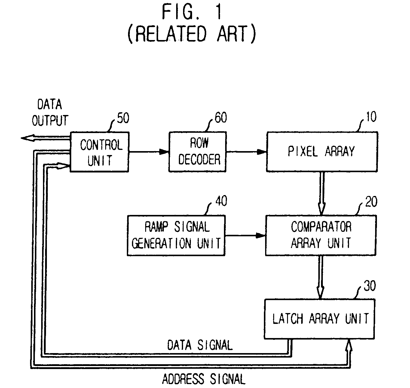
[0062] A complementary metal oxide semiconductor (CMOS) image sensor in accordance with a preferred embodiment of the present invention includes the same constitutional elements as the conventional CMOS image sensor shown in FIG. 1. Accordingly, since the constitutional elements of the CMOS image sensor are already explained in the description of the related arts, the explanations about the constitutional elements of the CMOS image sensor in accordance with the preferred embodiment of the present invention will be omitted herein.

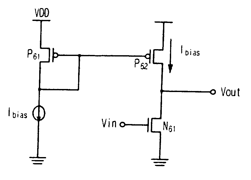
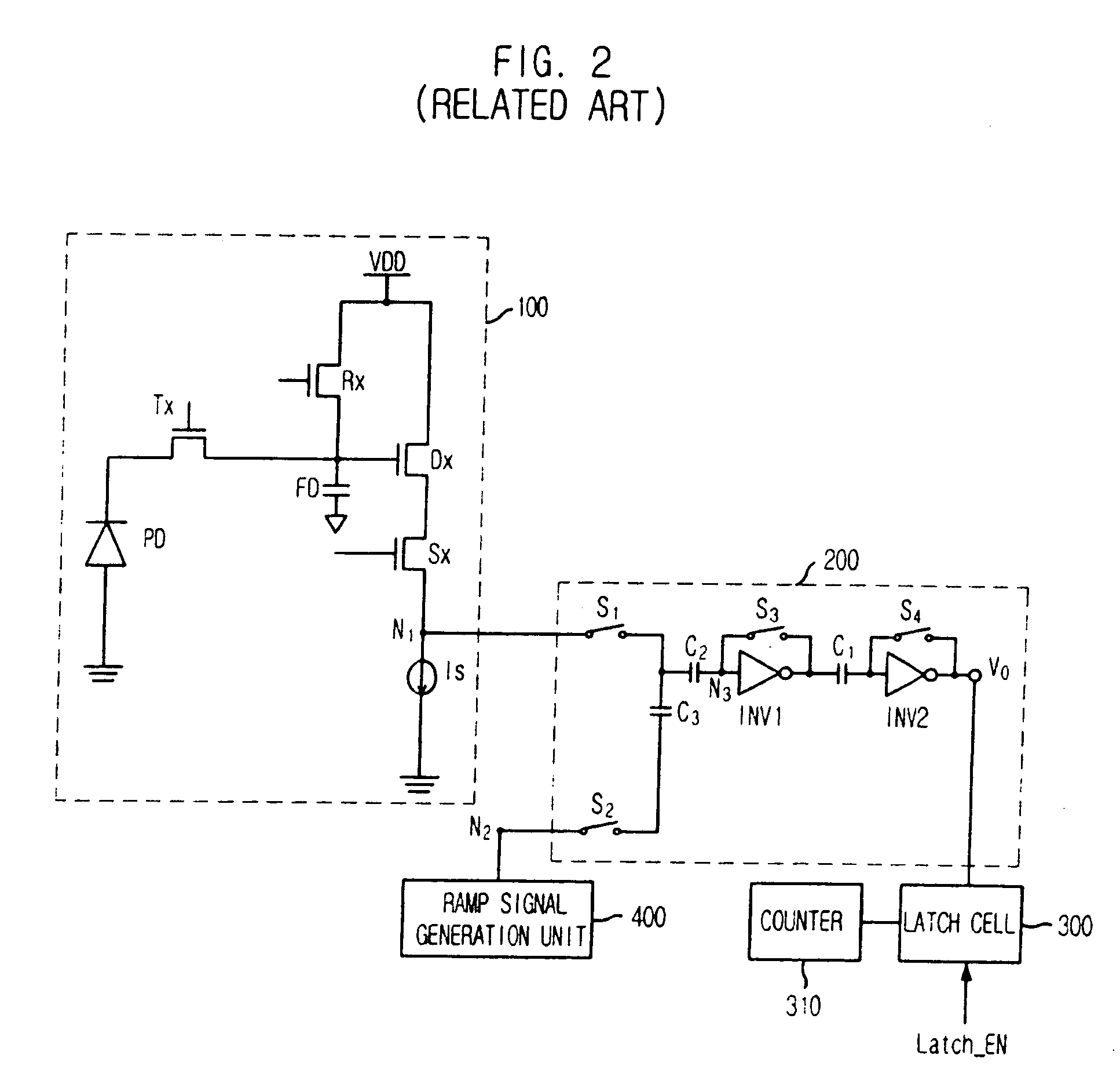
[0063] Furthermore, a path for converting a pixel value of a pixel to a digital signal and storing the converted digital signal, and waveforms illustrating a correlated double sampling (CDS) operation are identical to those shown in FIGS. 2 and 3. Thus, detailed explanations about the path and the CDS oper...


PUM


Abstract

A complementary metal oxide semiconductor (CMOS) image sensor capable of performing an analog correlated double sampling method is provided. The CMOS image sensor includes an image capturing unit for capturing an analog signal corresponding to an image of a subject; an analog-digital converting unit for converting the analog signal into a digital signal by using a ramp signal decreasing in a fixed slope according to a reference clock; a ramp signal generation unit for providing the ramp signal to the analog-digital converter; and a control unit for providing said units with control signals and outputting data to the outside through an interface.

Description

FIELD OF THE INVENTION [0001] The present invention relates to a complementary metal oxide semiconductor (CMOS) image sensor; and more particularly, to a CMOS image sensor capable of performing analog correlated double sampling. DESCRIPTION OF RELATED ARTS [0002] An image sensor is a device capturing an image by using a characteristic which a semiconductor reacts to the light. That is, in the image sensor, pixels detect different brightness and wavelengths of the light coming from a subject to thereby output the detected different brightness and wavelengths of the light as electrical values, and the electrical values are converted to voltage levels that can be subjected to a signal process. [0003] A charge coupled device (CCD) has been conventionally used as an image sensor. However, recently, a complementary metal oxide semiconductor (CMOS) image sensor is widely used because the CMOS image sensor can reduce power consumption and increase productivity by employing a CMOS process. [...

Claims


Application Information

Patent Timeline
IPC IPC(8): H03M1/12H04N5/357H04N5/374H04N5/378
CPCH03K19/0948H03M1/56H03M1/08H04N25/78E04G7/22E04G7/306E04G7/32E04G1/06
Inventor OH, HAEK-SOO
Owner INTELLECTUAL VENTURES II
Why Eureka
Try Eureka