Light emitting device and manufacturing method therefor

a technology of light emitting devices and manufacturing methods, which is applied in the manufacture of printed circuits, electric discharge lamps, envelopes/vessels, etc., can solve the problems of affecting the simplification affecting the efficiency of the manufacturing process, and using a material with high heat conductivity, etc., to achieve high heat radiation capacity, reduce heat conductivity, and high reliability

Inactive Publication Date: 2011-06-16
SEIKO INSTR INC
View PDF5 Cites 5 Cited by
  • Summary
  • Abstract
  • Description
  • Claims
  • Application Information

AI Technical Summary

Benefits of technology

[0013]According to the present invention, a heat radiating path without a part in which the heat conductivity is reduced may be secured, and hence it is possible to realize the light emitting device having high heat radiation capacity. Further, the reflecting member does not have porous structure, and hence it is possible to realize the highly-reliable light emitting device without a defect in sealing by the encapsulant.

Problems solved by technology

The above-mentioned LED package, however, does not use a material having high heat conductivity and hence an excellent heat radiation function as the board material.
Therefore, an excellent heat radiation effect cannot be obtained during the light emission operation of the LED element.
Further, the reflecting member is fixed to the board in a separate step, to thereby hinder simplification of the manufacturing process and hence increase assembly cost.
In addition, with the insulation layer 72 having porous structure and the encapsulant 76 covering the insulation layer 72, air bubbles are apt to be generated from the insulation layer part at the time when the encapsulant is formed, which leads to a problem of causing defects of incorporated air bubbles.
Therefore, when a material containing silver is used to fix the reflecting film and the LED element, there is another problem of accelerated degradation.

Method used


Image

  • Light emitting device and manufacturing method therefor
  • Light emitting device and manufacturing method therefor
  • Light emitting device and manufacturing method therefor

Examples


Embodiment Construction

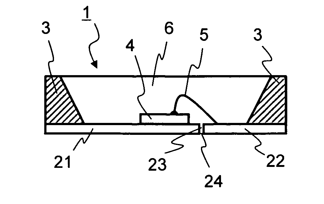
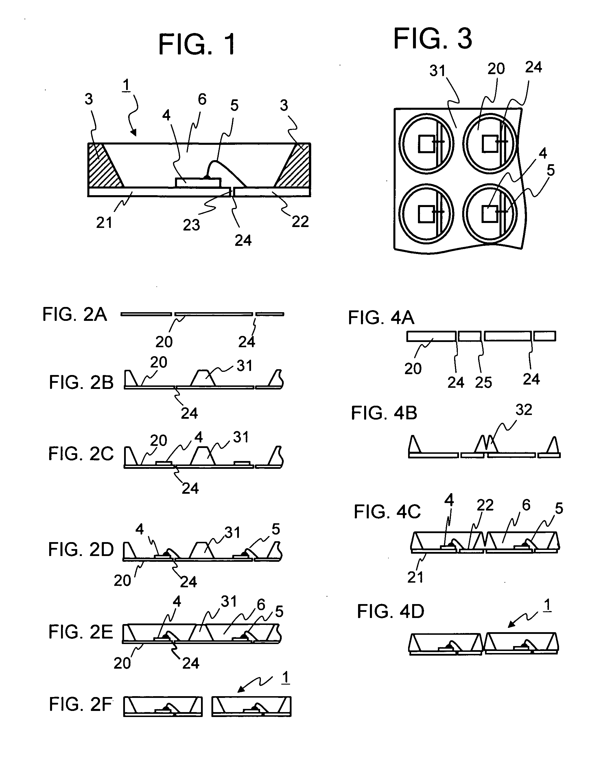
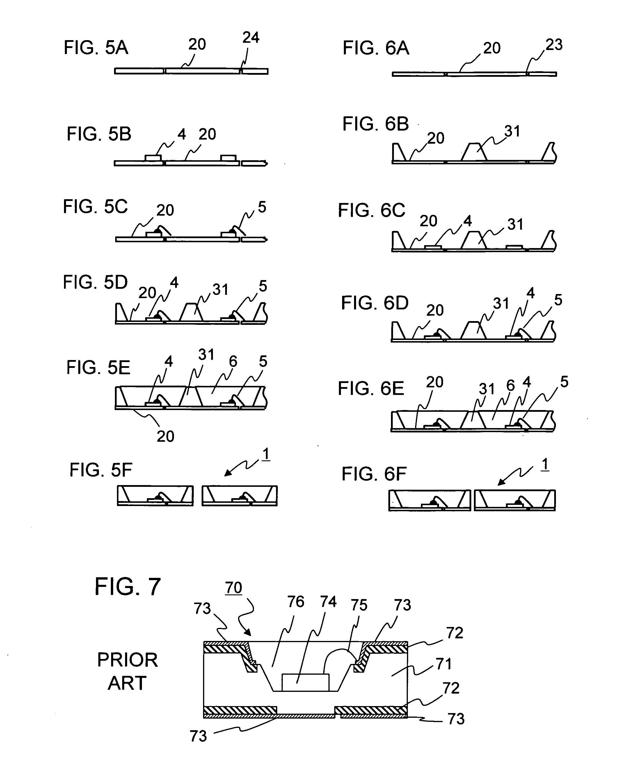
[0022]An embodiment of the present invention is described with reference to the attached drawings. FIG. 1 is a cross-sectional view illustrating a light emitting device 1 according to the present invention. The light emitting device 1 is constructed on the basis of a first metal substrate 21 and a second metal substrate 22 arranged across a slit 24. A light source 4 is mounted on the first metal substrate 21. The second metal substrate 22 is electrically connected to the light source 4 by a wire 5. The first metal substrate 21 and the second metal substrate 22 are insulated from each other by the slit 24. Further, a reflecting member 3 is placed on the first metal substrate 21 and the second metal substrate 22. An encapsulant 6 covers the light source 4. The slit 24 is filled with an insulating material 23 to maintain insulation between the first metal substrate 21 and the second metal substrate 22. A through hole is formed in the reflecting member 3. The through hole is inclined, a...


PUM

PropertyMeasurementUnit
thicknessaaaaaaaaaa
sizeaaaaaaaaaa
insulatingaaaaaaaaaa

Abstract

Provided is a highly-reliable light emitting device which has good heat radiation capacity and uses a light emitting diode (LED) having high luminance and high output as a light source. The light emitting device includes: the light source; a first metal substrate on which the light source is mounted; a wire connected to the light source; a second metal substrate electrically connected to the light source by the wire and formed on the same plane as the first metal substrate to be insulated from the first metal substrate; a planar reflecting member placed on the first metal substrate and the second metal substrate, having a through hole that is smaller in diameter on the light source side than on a side opposite to the light source side, and having a side surface formed of an inclined reflecting surface on the through hole side; an encapsulant for covering the light source; a slit formed between the first metal substrate and the second metal substrate; and an insulating material for filling the slit.

Description

BACKGROUND OF THE INVENTION[0001]1. Field of the Invention[0002]The present invention relates to a light emitting device which uses a light emitting diode (LED) element having high luminance and high output as a light source, and to a manufacturing method for the light emitting device. More specifically, the present invention relates to a light emitting device which is improved in heat radiation effect to thereby extend lifetime of an LED element.[0003]2. Description of the Related Art[0004]A conventional LED package is constructed by mounting an LED element serving as a light source on a patterned electrode of a circuit board, and integrally fixing a front surface of the board and a reflecting member having a reflecting surface, which passes through the reflecting member at an inclination angle, by epoxy resin or the like. The external size of the reflecting member is substantially the same as that of the board. In the LED package constructed as above, the reflecting surface reflec...

Claims


Application Information

Patent Timeline
Patent Type & Authority Applications(United States)
IPC IPC(8): H01K1/26H05K3/32
CPCH01L33/40H01L33/56H01L33/60H01L2933/0033Y10T29/49146H01L24/97H01L2224/48465H01L2224/48247H01L2224/48091H01L2924/12041H01L2924/00014H01L2924/00
Inventor NAKAMURA, TAKAHIKO
Owner SEIKO INSTR INC
Why Eureka
Try Eureka