Method for manufacturing of optoelectronic devices based on thin-film, intermediate-band materials description

Inactive Publication Date: 2011-06-16
UNIV MADRID POLITECNICA
View PDF4 Cites 3 Cited by
  • Summary
  • Abstract
  • Description
  • Claims
  • Application Information

AI Technical Summary

Problems solved by technology

This type of technology is highly material-demanding: either for an efficient absorption of electromagnetic (EM) radiation, like in silicon solar cells; or else due to the mere requirement of a solid and manageable substrate for subsequent processing.
A significant fraction of the overall production cost of this technology is thus simply associated to the material requirements.
Additional issues refer to the conditions for half-filling of the confined electronic states.
This type of growth, though commonly found, is not optimal for the manufacturing of the intended nanostructures, which would require complete three-dimensional

Method used


Image

  • Method for manufacturing of optoelectronic devices based on thin-film, intermediate-band materials description
  • Method for manufacturing of optoelectronic devices based on thin-film, intermediate-band materials description

Examples


Embodiment Construction

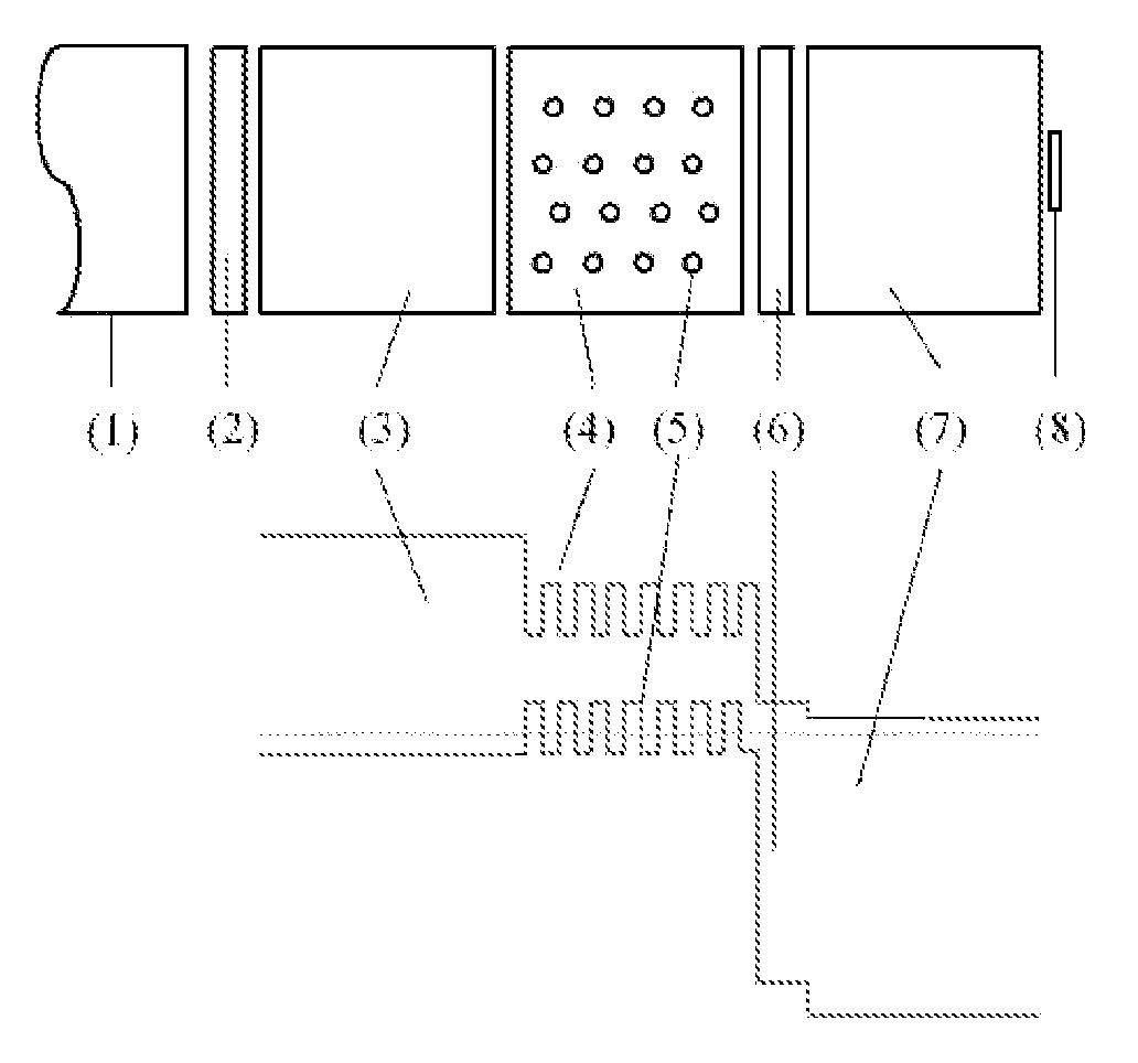
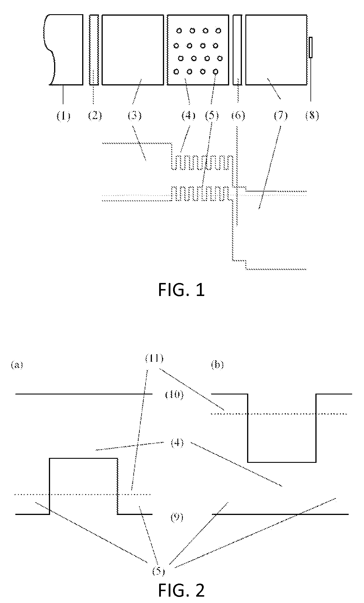
[0012]The present invention refers to the manufacturing of optoelectronic devices based on thin-film IBMs, starting from a manufacturing procedure of nanoscopic structures of multinary compounds of the chalcopyrite type, e.g., (Cu,Ag)(Al,Ga,In)(S,Se,Te)2 and derivatives obtained from deviations in the stoichiometry, the so-called I-III3-VI5 and I-III5-VI8 compounds, as described before (DE 102006060366.4-43, Phys. Rev. B 77, 085315, 2008). According to the referred procedure, it is possible to embed nanoscopic structures inside a semiconducting matrix in a single technological process, resulting in an IBM. The novelty of the design lies in the incorporation of such a procedure into the typical processing sequence of thin-film devices, by which thin-film intermediate band solar cells can be obtained.

[0013]This structure is formally analog to that described in the literature as an IBM obtained from epitaxial growth of III-V compounds. However, the method proposed has a number of advan...


PUM


Abstract

Method for manufacturing of optoelectronic devices based on thin-film, intermediate band materials, characterized in that it comprises, at least, the following steps:
a first stage wherein a substrate (1) is coated with a metal layer acting as electrode (2);
a second stage, whereby atop the metal layer (2) a p-type semiconductor (3) is deposited; and
a third stage, whereby the intermediate band material is processed;
and wherein such an intermediate band material comprises nanoscopic structures (4) of multinary material of the type (Cu,Ag)(Al,Ga,In)(S,Se,Te)2 embedded in a matrix (5) of a similar composition, except for the absence of, at least, one cationic species present in the nanostructure.

Description

FIELD OF THE INVENTION[0001]The present invention refers to a method for manufacturing of a type of opto-electronic device, which is based on the characteristic properties of intermediate band materials and adapted for its realization utilizing technological processes devised for thin-film technologies, with particular emphasis on multinary materials of the chalcopyrite type.PRIOR ART[0002]Commercial photovoltaic solar cells can be classified into three main categories, according to their manufacturing technologies. The so-called first-generation technology, currently dominating the PV-market, refers to wafer-based solar cells, typically single- or multi-crystalline silicon, as well as single-junction solar cells based on III-V semiconducting compounds (e.g. GaAs, InP, etc.). This type of technology is highly material-demanding: either for an efficient absorption of electromagnetic (EM) radiation, like in silicon solar cells; or else due to the mere requirement of a solid and manage...

Claims


Application Information

Patent Timeline
IPC IPC(8): H01L33/26H01L31/18H01L31/0256B82Y99/00
CPCH01L31/0322H01L31/0336Y02E10/541H01L31/03923H01L31/035209Y02P70/50H01L31/06H01L31/035218H01L31/042
Inventor FUERTES MARRON, DAVIDMARTI VEGA, ANTONIOLUQUE LOPEZ, ANTONIO
Owner UNIV MADRID POLITECNICA
Why Eureka
Try Eureka