Inorganic light-emitting device

a light-emitting device and inorganic technology, applied in the direction of discharge tube luminescnet screens, discharge tube/lamp details, electric discharge lamps, etc., can solve the problems of low light emission brightness, high driving voltage, and limitations of light-emitting devices, and achieve high and overall uniform light emission efficiency, long life, and high mechanical strength

Inactive Publication Date: 2011-06-23
KYONGGI UNIV IND & ACAD COOPERATION FOUND
View PDF5 Cites 10 Cited by
  • Summary
  • Abstract
  • Description
  • Claims
  • Application Information

AI Technical Summary

Benefits of technology

[0013]In the inorganic light emitting device according to the present invention, the fluorescent layer is uniformly formed by coating nanowires formed of an inorganic light emitting material or the nanowires together with an organic material, high and overall uniform light emission efficiency can be maintained.
[0014]Also, the fluorescent layer of the inorganic light emitting device is formed of nanowires formed of an inorganic light emitting material, and thus the inorganic light emitting device can realize high mechanical strength and long lifetime and can maintain overall uniform and high light emission efficiency.
[0015]Also, the fluorescent layer of the inorganic light emitting device is formed of nanowires, and thus when the inorganic light emitting device is driven by a low voltage, electrons are overall uniformly excited in the fluorescent layer, thereby realizing high light emission brightness.
[0016]Also, since the fluorescent layer of the inorganic light emitting device is formed of nanowires unlike in a conventional fluorescent layer that is formed as a flat panel type thin film, the fluorescent layer has transparency and physical flexibility. Thus, the fluorescent layer can be used as a light emitting device or a backlight of a flat panel display apparatus.

Problems solved by technology

However, the light emitting device also has some limitations that it requires a high driving voltage, has low light emission brightness, and is difficult to realize a blue color.
However, a light emitting device having a fluorescent layer formed of an organic fluorescent material has high light emission efficiency and a low driving voltage.
However, it has low thermal stability and a short lifetime.

Method used


Image

  • Inorganic light-emitting device
  • Inorganic light-emitting device
  • Inorganic light-emitting device

Examples


Embodiment Construction

[0035]Inorganic light emitting devices according to embodiments of the present invention win now be described more fully hereinafter with reference to the accompanying drawings.

[0036]First, an inorganic light emitting device according to an embodiment of the present invention will be described.

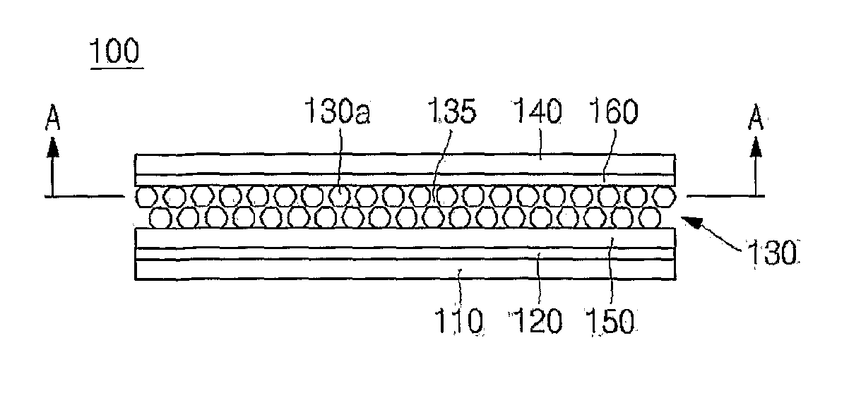
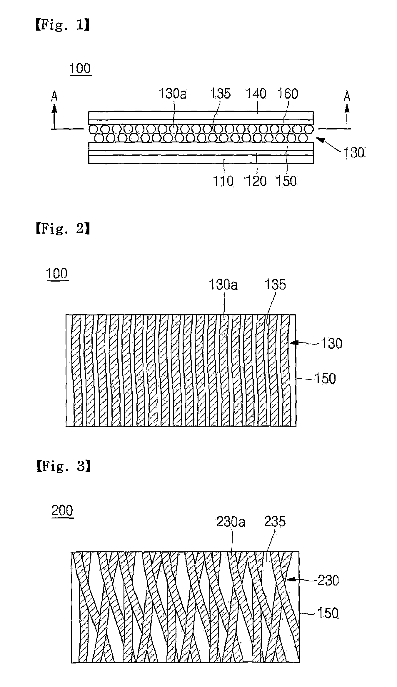
[0037]FIG. 1 is a schematic vertical cross-sectional view of an inorganic light emitting device 100 according to an embodiment of the present invention. FIG. 2 is a schematic plan view taken along a line A-A of FIG. 1.

[0038]Referring to FIGS. 1 and 2, the inorganic light emitting device 100 according to an embodiment of the present invention may include a first electrode 120, a fluorescent layer 130, and a second electrode 140. Also, the inorganic light emitting device 100 may further include a substrate 110 formed on a lower surface of the first electrode 120. Also, the inorganic light emitting device 100 may further include a first insulating layer 150 formed between the first electrode 120 ...


PUM

PropertyMeasurementUnit
thicknessaaaaaaaaaa
diameteraaaaaaaaaa
thicknessaaaaaaaaaa

Abstract

The present invention relates to an inorganic light-emitting device, and more particularly, to an inorganic light emitting device having superior mechanical strength and a long lifespan, and which is capable of maintaining uniform and high efficiency of light emission, and has transparent and flexible characteristics. The inorganic light emitting device of the present invention includes a first electrode, a fluorescent layer formed on the first electrode, and which includes a plurality of nanowires made of inorganic light-emitting materials, and a second electrode formed on the fluorescent layer. The fluorescent layer is coated with the plurality of nanowires.

Description

TECHNICAL FIELD[0001]Embodiments relate to inorganic light emitting devices that can be used for light emitting devices or backlights of flat panel display apparatuses.BACKGROUND ART[0002]A light emitting device includes a fluorescent layer formed between first and second electrodes, and the fluorescent layer is formed of a fluorescent material that includes an organic fluorescent material or an inorganic fluorescent material. When a voltage is applied between the first and second electrodes, the fluorescent material included in the fluorescent layer is excited, and thus the light emitting device emits visible light. The light emitting device is used as a light emitting diode of a flat panel display such as plasma display panel (PDP) or an organic light emitting diode (OLED), or a backlight of a liquid crystal display apparatus.[0003]In a light emitting device that includes the fluorescent layer formed of an inorganic fluorescent material, the inorganic fluorescent material is in a ...

Claims


Application Information

Patent Timeline
Patent Type & Authority Applications(United States)
IPC IPC(8): H01J1/63H01J1/62
CPCH05B33/145
Inventor JU, SANG HYUN
Owner KYONGGI UNIV IND & ACAD COOPERATION FOUND
Why Eureka
Try Eureka