Electroactive Optical Device

a piezoelectric crystal and optical element technology, applied in the field of electroactive optical devices, can solve the problems of poor application suitability, comparatively high manufacturing cost, and poor application suitability of devices based on piezoelectric crystals, and achieve the effects of large deformation, easy manufacturing process, and strong change of the curvature of the surface of the optical elemen

Inactive Publication Date: 2011-06-23
OPTOTUNE CONSUMER AG
View PDF4 Cites 45 Cited by
  • Summary
  • Abstract
  • Description
  • Claims
  • Application Information

AI Technical Summary

Benefits of technology

[0011]By varying the axial extension of the two regions and thereby radially displacing material of the optical element, a strong change of the curvature of the surface of the optical element can be achieved.
[0012]This design uses the advantages of an electroactive actuator, such as its potentially easy manufacturing process, large deformations and low actuation voltage, while providing a solution that has a long lifetime because, in the absence of a voltage, the device is in an elastically relaxed state and therefore is less p...

Problems solved by technology

Devices based on piezoelectric crystals are, however, comparatively expensive to manufacture.
Due to the high voltage required to control this device, it is poorly suited for many applications.
Also, prior art devices of these types often ...

Method used


Image

  • Electroactive Optical Device
  • Electroactive Optical Device
  • Electroactive Optical Device

Examples


Embodiment Construction

Definitions

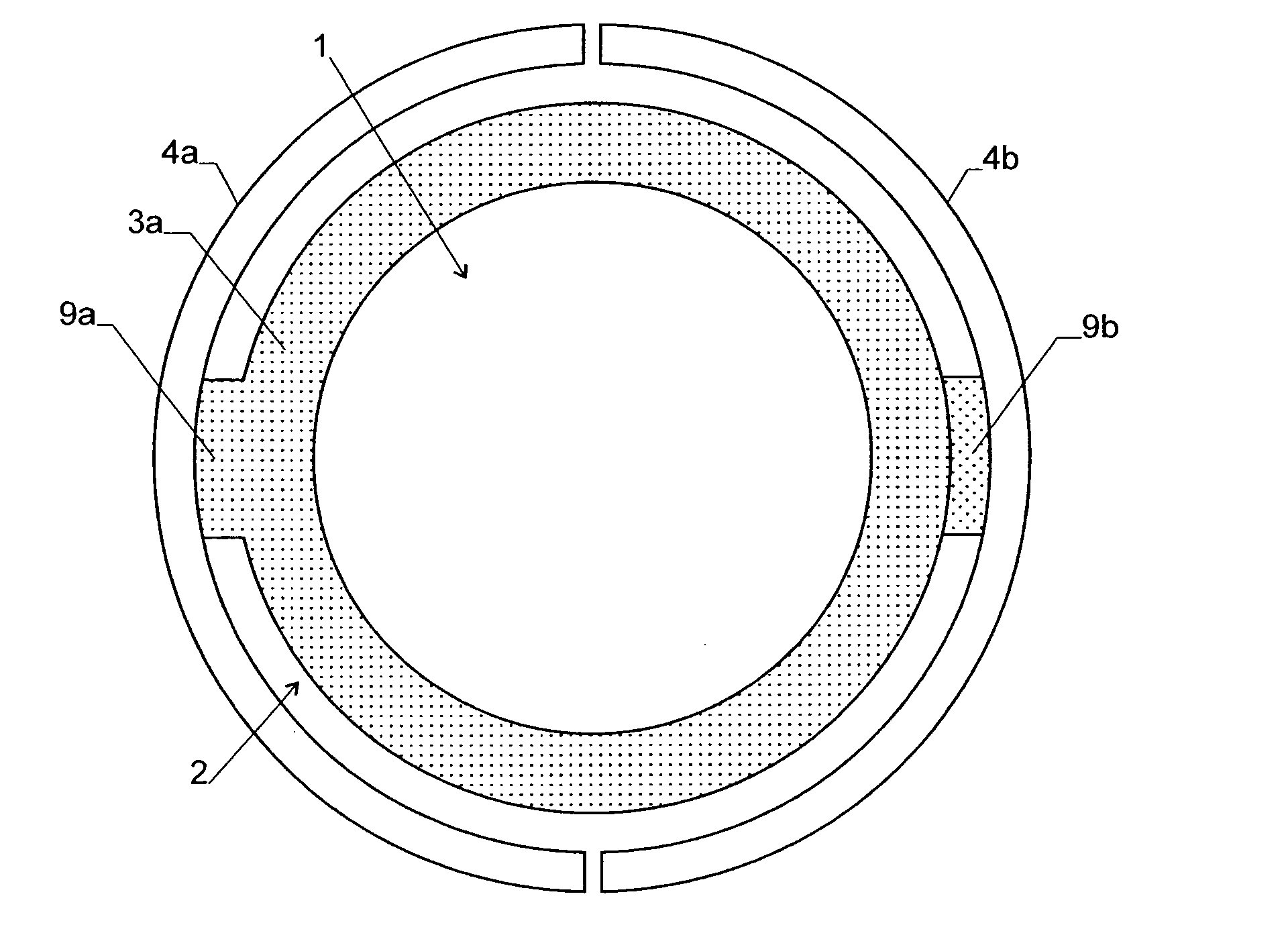
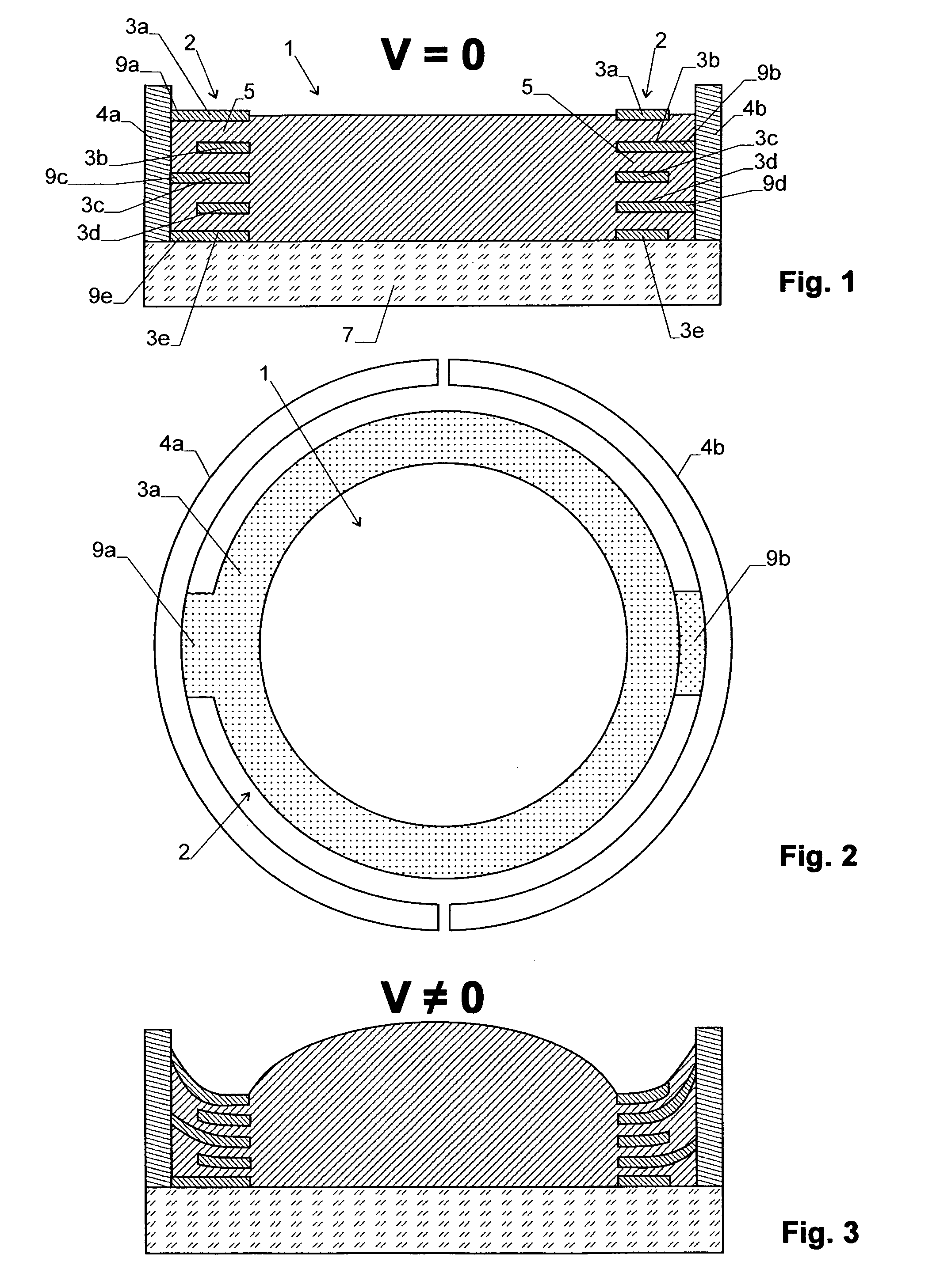
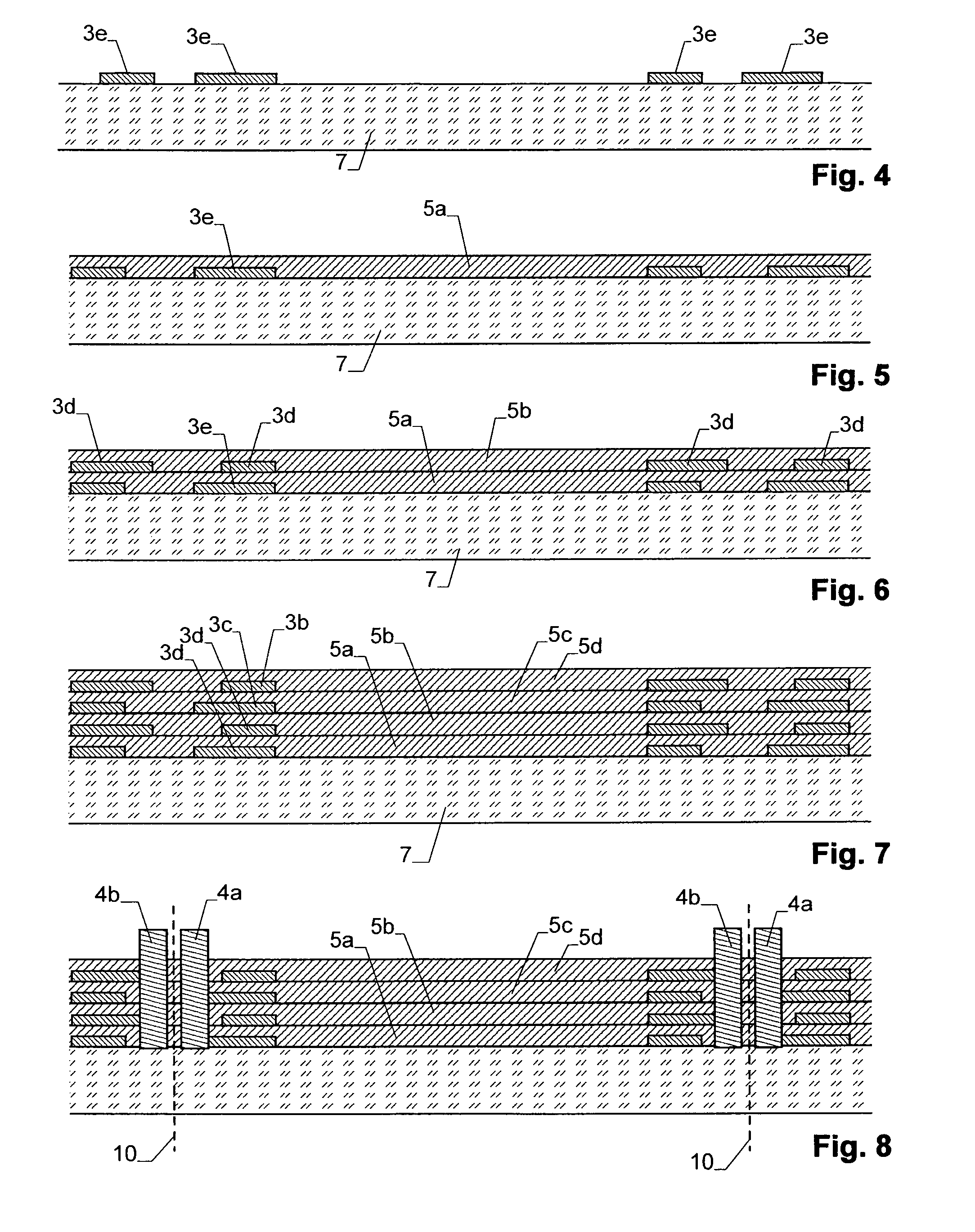
[0040]The term “axial” is generally used to designate a direction perpendicular to the surface of the center region of the optical element in its relaxed state. If a substrate is present, the substrate will in most cases be aligned perpendicularly to the axial direction.

[0041]The term “radial” is used to designate a direction perpendicular to the axial direction.

[0042]Introduction

[0043]The present invention can be implemented in a variety of forms, e.g. as an electroactive lens, a beam deflector or an anti-jittering device. In the following, we describe some of these applications.

[0044]Electroactive Lenses

[0045]One possible embodiment of the present invention as an electroactive lens is shown in FIGS. 1 and 2. The lens comprises an elastic optical element 1 and an electroactive element 2. In the present embodiment, the optical element 1 is circular and the electroactive element 2 surrounds the optical element. However, as mentioned below, the present invention can also be...


PUM

PropertyMeasurementUnit
Diameteraaaaaaaaaa
Volumeaaaaaaaaaa
Electrical conductoraaaaaaaaaa

Abstract

An electroactive optical device, in particular an electroactive lens, comprising an optical element (1) as well as an electroactive element (2) is described. The optical element (1) is an elastic solid, such as a gel or a polymer. The electroactive element (2) comprises a plurality of compliant electrodes (3a-3e) stacked on top of each other with an electroactive material (5) between them. The electroactive element (2) is surrounded by a rigid wall (4a, 4b), which provides two common contacts for the electrodes (3a-3e). In the absence of an applied electric voltage, the optical element (1) is in a mechanically relaxed State, which reduces undesired ageing effects. Upon application of a voltage to the electrodes (3a-3e) the optical element (2) is deformed.

Description

TECHNICAL FIELD[0001]The invention relates to an electroactive optical device, in particular an electroactive lens, as well as to a method for manufacturing such a device.BACKGROUND ART[0002]An electroactive optical device is an optical device whose shape can be changed using the electroactive effect. In particular, an electroactive optical lens is a lens whose focal length can be changed using the electroactive effect.[0003]The term electroactive effect describes an electric-field induced deformation of a solid or liquid. The deformation can be due to Coulomb forces between electrodes and / or due to the rearrangement of electrical ions and / or multipoles, in particular dipoles, in an electric field. Examples of electroactive materials are: dielectric elastomers, electrostrictive relaxor ferroelectric polymers, piezoelectric polymers (PVDF), liquid crystal elastomers (thermal), ionic polymer-metal composites, mechano-chemical polymers / gels.[0004]A variety of electroactive lens designs...

Claims


Application Information

Patent Timeline
IPC IPC(8): G02B3/14H05K13/00
CPCG02B3/14Y10T29/49117Y10T29/49002G02B26/005G02B3/00H02N2/02G02B7/28H10N30/00
Inventor BLUM, MARK
Owner OPTOTUNE CONSUMER AG
Why Eureka
Try Eureka