

Package structure having micro-electromechanical element and fabrication method thereof
- Summary
- Abstract
- Description
- Claims
- Application Information
AI Technical Summary
Benefits of technology
Problems solved by technology
Method used
Image

Examples
first preferred embodiment
[0035]FIG. 2A through FIG. 2H are cutaway views illustrating a first embodiment of the package structure having the micro-electromechanical (MEMS) element and a fabrication method thereof according to the present invention, wherein FIG. 2F is a top view and FIG. 2F′ is a cutaway view of FIG. 2F;
[0036]As shown in FIG. 2A, a wafer 20 is provided whereon a plurality of electrical connecting pads 201 and a plurality of the MEMS elements 202 are formed, wherein the wafer 20 may be made of a silicon material, and the MEMS elements include gyroscopes, accelerometers or radiation frequency (RF MEMS) elements.
[0037]As illustrated in FIG. 2B, a plurality of lids 21 are disposed on the wafer 20 each covering on a MEMS element 202, wherein the lids 21 may be formed by glass or silicon materials.
[0038]As shown in FIG. 2C, a stud bump 22 is formed on each of the electrical connecting pads 201, wherein the stud bump 22 is made of a metallic material, and preferably, a soldering material such as Go...
second preferred embodiment
[0048]FIG. 3 is a cutaway view illustrating a second embodiment of the package structure having the MEMS element according to the present invention. In this embodiment, the package structure 3 is similar to the one depicted in FIG. 2H and only differs in that the protruding portion 233 of the encapsulant 23 formed on the MEMS element 202 is provided with an encapsulant opening 232 for allowing the MEMS element 202 to be exposed therefrom. The fabrication method of the package structure 3 is substantially identical to that of the first embodiment and the description thereof is omitted herein for brevity.
third preferred embodiment
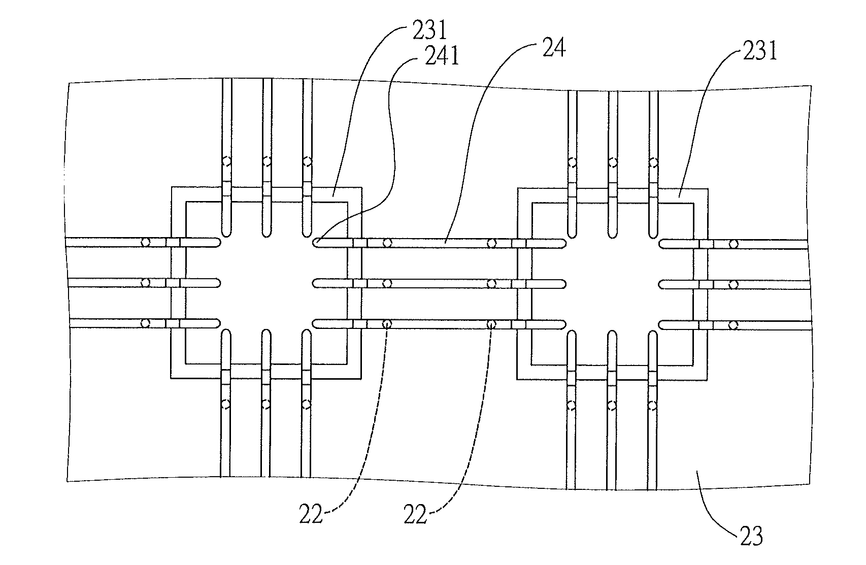
[0049]FIG. 4 is a cutaway view illustrating a third embodiment of the package structure having the MEMS element according to the present invention. In this embodiment, the package structure 4 is similar to the one depicted in FIG. 3 and only differs in that the metal conductive layer 24 is formed to extend to the lid 21 in the encapsulant opening 232, and the contact pads 241 are formed on the lid 21. The fabrication method of the package structure 4 is substantially identical to that of the first embodiment and the description thereof is omitted herein for brevity.
PUM
 Abstract
Description
Claims
Application Information