Dielectric film growth with radicals produced using flexible nitrogen/hydrogen ratio

a technology of dielectric film and nitrogen, which is applied in the direction of electric discharge tubes, coatings, chemical vapor deposition coatings, etc., can solve the problems of dielectric material, dielectric material, and structural features of the device having decreased spatial dimensions, and achieves the effect of greater flexibility

Active Publication Date: 2011-06-30
APPLIED MATERIALS INC
View PDF101 Cites 37 Cited by
  • Summary
  • Abstract
  • Description
  • Claims
  • Application Information

AI Technical Summary

Benefits of technology

[0007]Embodiments of the invention include methods of forming a dielectric layer on a substrate in a plasma-free substrate processing region in a substrate processing chamber. The methods include flowing a nitrogen-and-hydrogen-containing gas into a plasma region to produce a radical-nitrogen precursor. The nitrogen-and-hydrogen-containing gas includes hydrogen (H2) and nitrogen (N2) allowing greater flexibility in choosing a nitrogen:hydrogen atomic flow ratio into the plasma region. The methods further include combining a silicon-containing precursor with the radical-nitrogen precursor in the plasma-free substrate processing region and depositing the dielectric layer on the substrate.

Problems solved by technology

The decreasing feature sizes result in structural features on the device having decreased spatial dimensions.
The widths of gaps and trenches on the device narrow to a point where the aspect ratio of gap depth to its width becomes high enough to make it challenging to fill the gap with dielectric material.
The depositing dielectric material is prone to clog at the top before the gap completely fills, producing a void or seam in the middle of the gap.
However, once these highly flowable materials are deposited, they have to be hardened into a solid dielectric material.
Unfortunately, the departing carbon and hydroxyl species often leave behind pores in the hardened dielectric that reduce the quality of the final material.
In addition, the hardening dielectric also tends to shrink in volume, which can leave cracks and spaces at the interface of the dielectric and the surrounding substrate.

Method used


Image

  • Dielectric film growth with radicals produced using flexible nitrogen/hydrogen ratio
  • Dielectric film growth with radicals produced using flexible nitrogen/hydrogen ratio
  • Dielectric film growth with radicals produced using flexible nitrogen/hydrogen ratio

Examples


Embodiment Construction

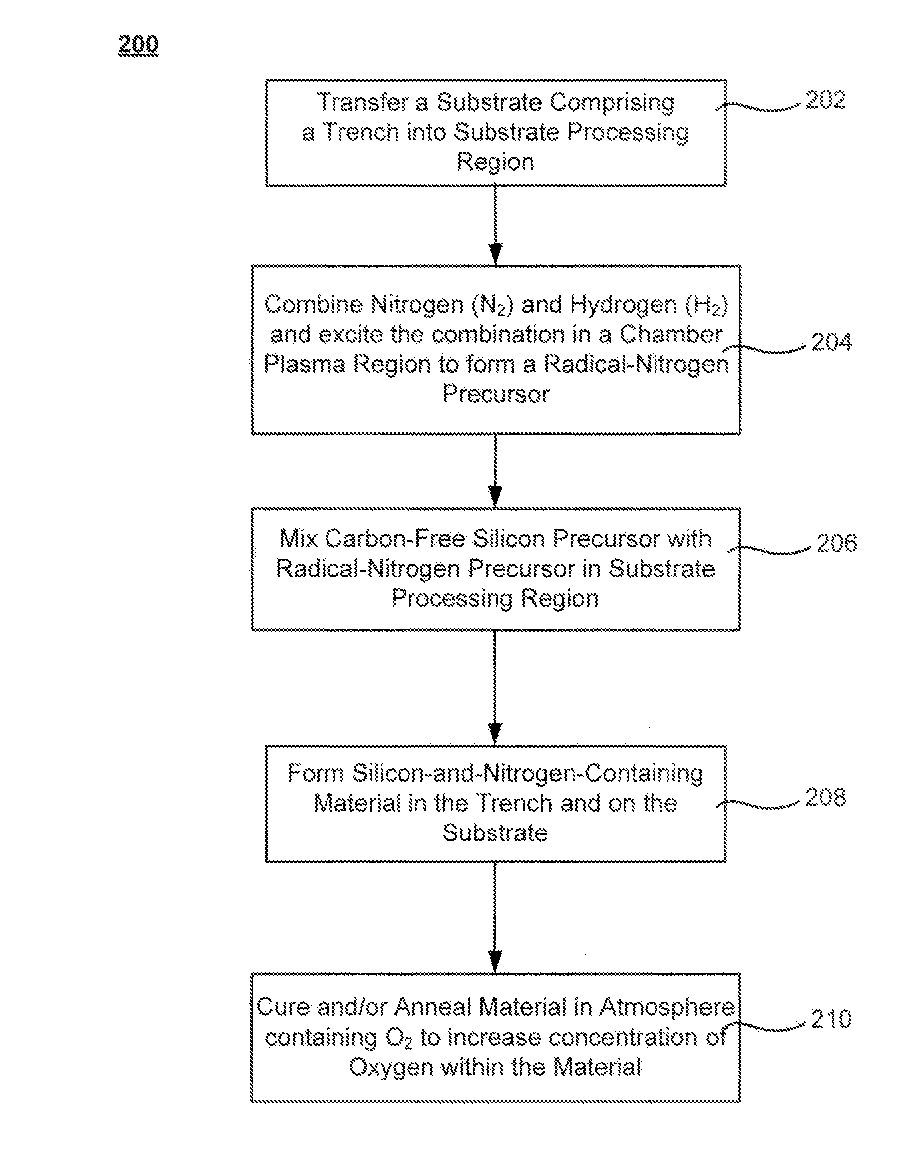
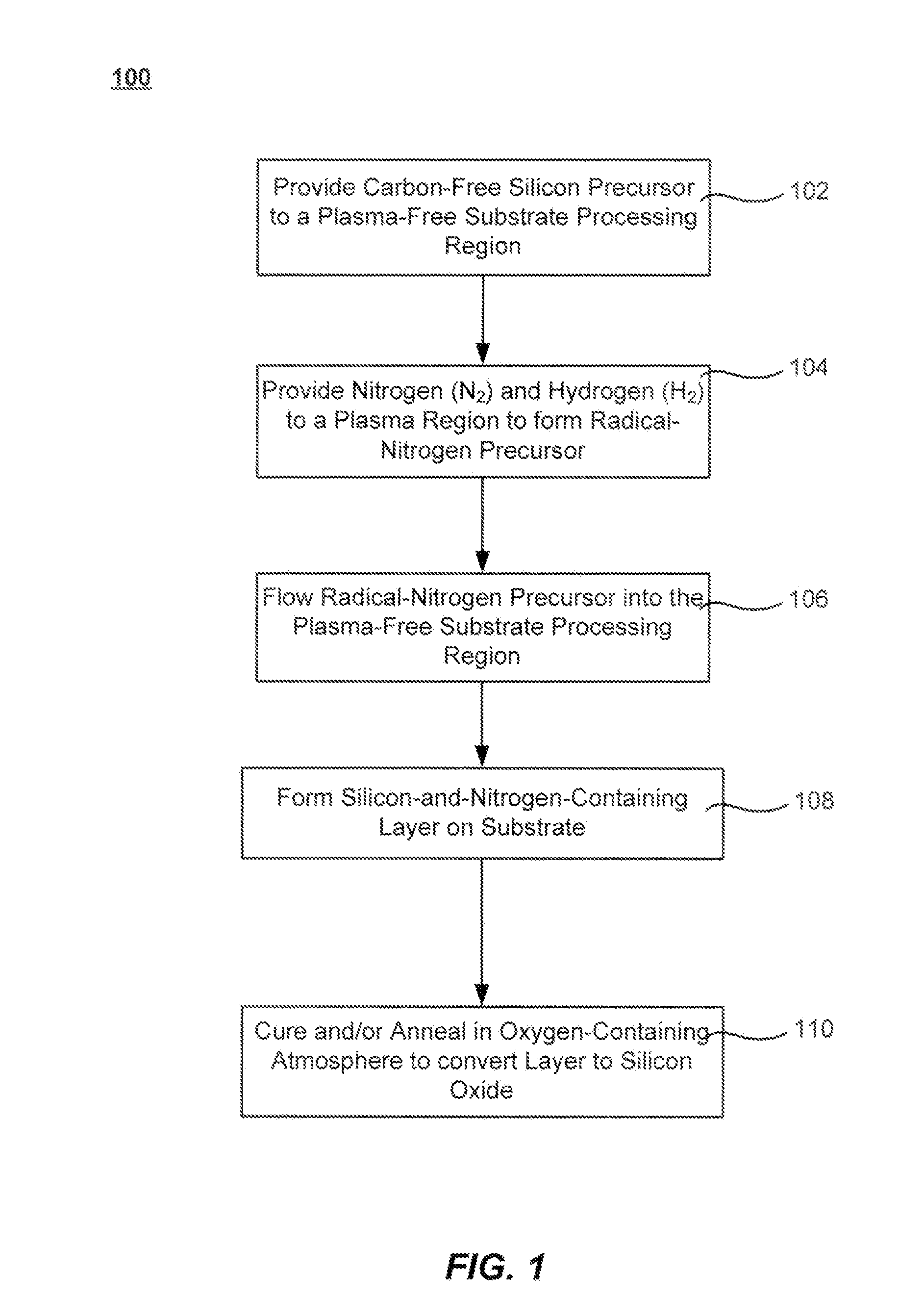
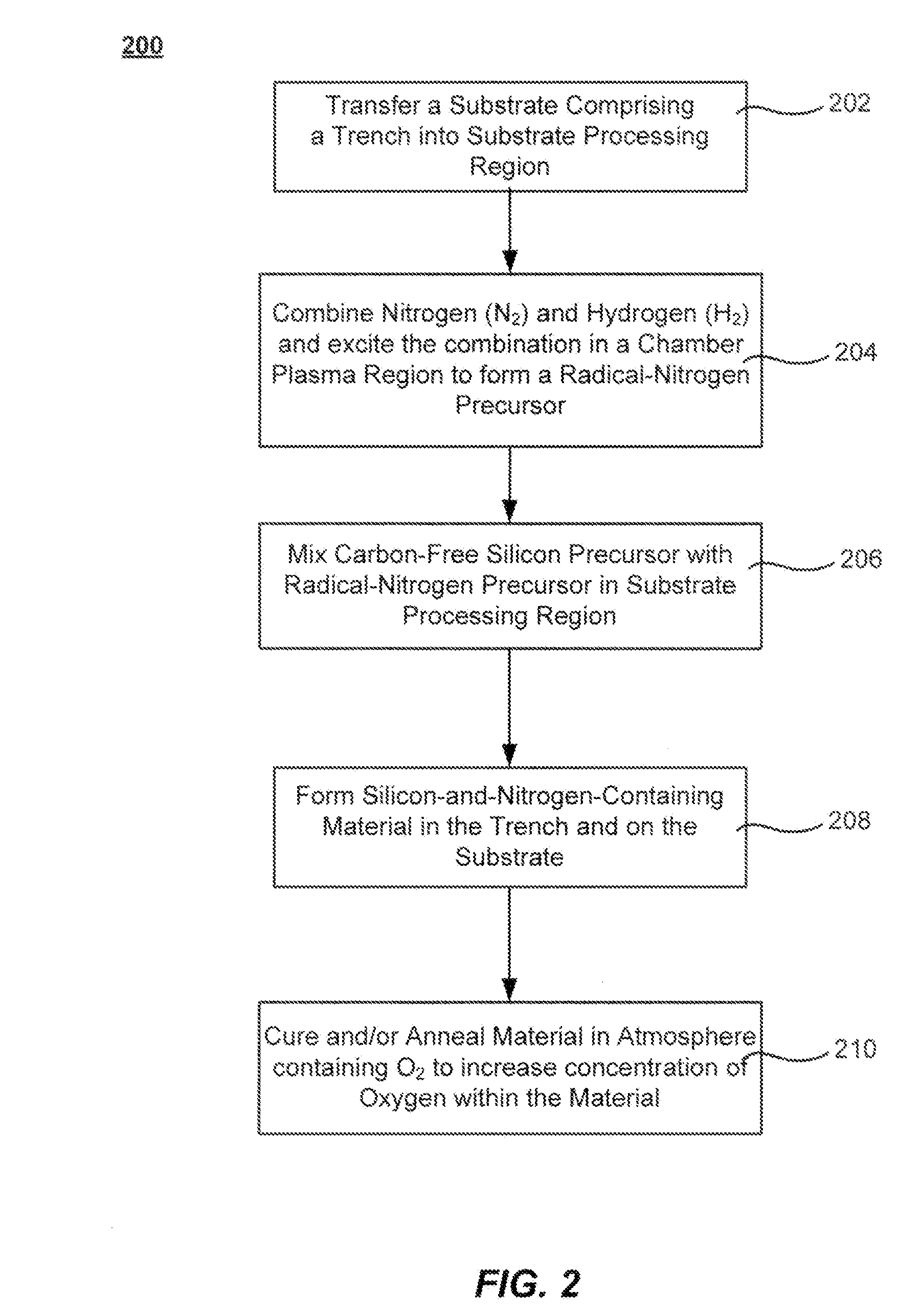
[0015]Methods of forming dielectric layers are described. The method may include the steps of mixing a silicon-containing precursor with a radical-nitrogen precursor, and depositing a dielectric layer on a substrate. The radical-nitrogen precursor is formed in a remote plasma by flowing hydrogen (H2) and nitrogen (N2) into the plasma in order to allow adjustment of the nitrogen / hydrogen ratio. The dielectric layer is initially a silicon-and-nitrogen-containing layer which may be converted to a silicon-and-oxygen-containing layer by curing and / or annealing the film in an oxygen-containing environment.

[0016]Increasing the concentration of nitrogen used to form the radical-nitrogen precursor reduces nascent flowability but generally produces a higher film quality (e.g. higher density, less shrinkage). On the other hand, decreasing the concentration of nitrogen increases the nascent flowability during deposition at the expense of film quality. Following the deposition, the silicon-and-n...


PUM

PropertyMeasurementUnit
temperatureaaaaaaaaaa
widthaaaaaaaaaa

Abstract

Methods of forming dielectric layers are described. The method may include the steps of mixing a silicon-containing precursor with a radical-nitrogen precursor, and depositing a dielectric layer on a substrate. The radical-nitrogen precursor is formed in a remote plasma by flowing hydrogen (H2) and nitrogen (N2) into the plasma in order to allow adjustment of the nitrogen/hydrogen ratio. The dielectric layer is initially a silicon-and-nitrogen-containing layer which may be converted to a silicon-and-oxygen-containing layer by curing and/or annealing the film in an oxygen-containing environment.

Description

CROSS-REFERENCES TO RELATED APPLICATIONS[0001]This application claims the benefit of U.S. Prov. Pat. App. No. 61 / 291,054 filed Dec. 30, 2009, and titled “NITRIDE FILM GROWTH WITH RADICALS PRODUCED USING FLEXIBLE NITROGEN / HYDROGEN RATIO,” which is entirely incorporated herein by reference for all purposes.BACKGROUND OF THE INVENTION[0002]Semiconductor device geometries have dramatically decreased in size since their introduction several decades ago. Modern semiconductor fabrication equipment routinely produces devices with 45 nm, 32 nm, and 28 nm feature sizes, and new equipment is being developed and implemented to make devices with even smaller geometries. The decreasing feature sizes result in structural features on the device having decreased spatial dimensions. The widths of gaps and trenches on the device narrow to a point where the aspect ratio of gap depth to its width becomes high enough to make it challenging to fill the gap with dielectric material. The depositing dielectr...

Claims


Application Information

Patent Timeline
Patent Type & Authority Applications(United States)
IPC IPC(8): H01L21/31
CPCC23C16/345C23C16/452C23C16/56H01J37/32357H01L21/02337H01L21/0217H01L21/02274H01L21/02326H01L21/02164H01L21/02109H01L21/02205
Inventor LIANG, JINGMEICHEN, XIAOLINMILLER, MATTHEW L.INGLE, NITIN K.VENKATARAMAN, SHANKAR
Owner APPLIED MATERIALS INC
Why Eureka
Try Eureka