Lead frame substrate, manufacturing method thereof, and semiconductor apparatus

a manufacturing method and semiconductor technology, applied in semiconductor devices, electrical devices, semiconductor/solid-state device details, etc., can solve the problems of complex steps of substrates, increased costs, and inability to keep up with the number of electrodes of lead frame types, so as to increase the number of terminals of semiconductor elements, secure thermal stress resistance, and stable connection

Inactive Publication Date: 2011-07-07
TOPPAN PRINTING CO LTD
View PDF8 Cites 16 Cited by
  • Summary
  • Abstract
  • Description
  • Claims
  • Application Information

AI Technical Summary

Benefits of technology

[0019]The present invention has been achieved in view of the aforementioned problems in the prior art, and has an object to provide: a lead frame substrate capable of supporting an increase in the number of the electrodes of a semiconductor element, high in reliability, and stable in its fabrication and assembly of a semiconductor package; a manufacturing method of the lead frame substrate; and a semiconductor apparatus.
[0023]According to the present invention, it is possible to arrange external connection terminals for connection with a printed wiring board in an array over a whole rear surface of a lead frame substrate. Therefore, it is possible to support an increased number of terminals of a semiconductor element.
[0024]Furthermore, the present invention includes a substrate based on a lead frame without using plated conducting wires. Therefore, it is possible to secure reliability against thermal stress.
[0025]On the other hand, in fabrication of such a lead frame substrate, no faults such as breakage or bending of a conducting wire occur. At the time of wire bonding performed in the assembly step of the semiconductor package, the lower portion of the wire-bonding connection terminal has the pre-mold resin filled uniformly on the surfaces of the external connection terminals, allowing for stable connection.

Problems solved by technology

In recent years, with the increase in the number of electrodes of a semiconductor element, semiconductor packages of a lead frame type that has outer leads on the side surfaces have become incapable of keeping up with the number of electrodes.
However, this poses the following problems.
The manufacture of such substrates has complex steps, leading to higher costs.
In addition, reliability is inferior to that of the packages of a lead frame type because plating is used for wiring connections within the substrate.

Method used


Image

  • Lead frame substrate, manufacturing method thereof, and semiconductor apparatus
  • Lead frame substrate, manufacturing method thereof, and semiconductor apparatus
  • Lead frame substrate, manufacturing method thereof, and semiconductor apparatus

Examples


examples

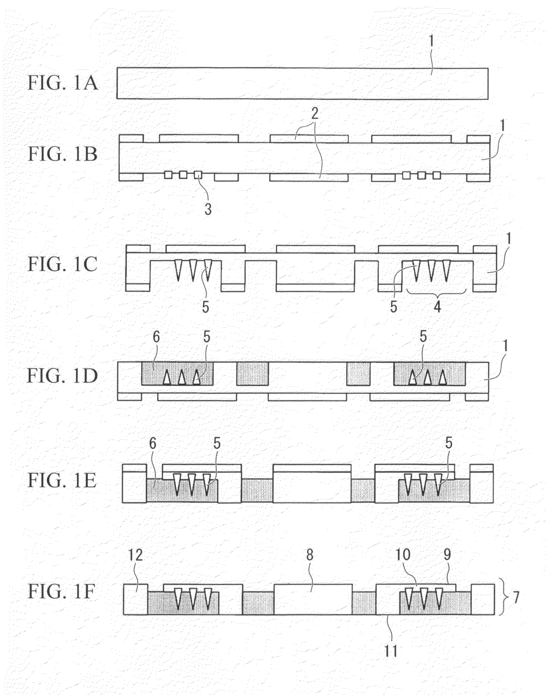
[0055]Hereunder is a description of an exemplary manufacturing method of a lead frame substrate according to the present invention with reference to FIG. 1A to FIG. 1F, taking an LGA (Land Grid Array) type lead frame substrate by way of example.

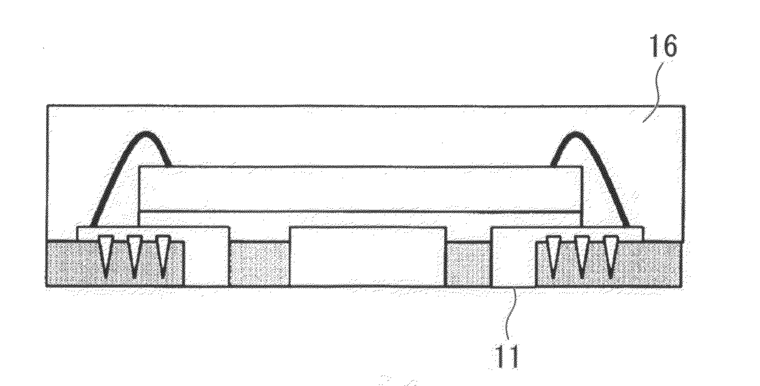
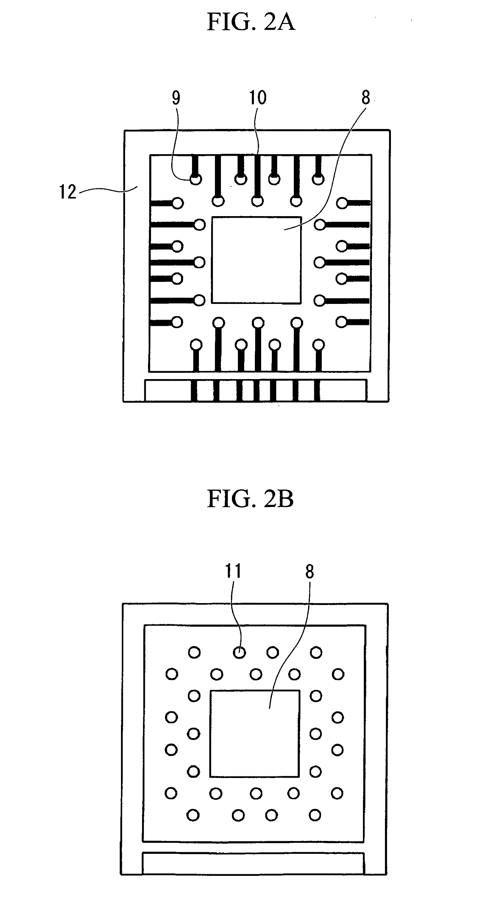
[0056]The manufactured LGA had a package size of 10 mm square. The bottom surface of the package had 168 external connection terminals arranged in an array.

[0057]First, a metal plate 1 shown in FIG. 1A was prepared, which was a long, band-like metal plate made of copper alloy (EFTEC64T manufactured by FURUKAWA ELECTRIC CO., LTD) with a width of 150 mm and a thickness of 200 μm.

[0058]Subsequently, on both surfaces of the metal plate 1, a photoresist (OFPR4000 manufactured by TOKYO OHKA KOGYO CO., LTD.) was coated with a roll coater so as to have a thickness of 5 μm. Then, the metal plate 1 was pre-baked at 90° C.

[0059]Next, the metal plate 1 was pattern-exposed from both sides via photo masks with desired patterns. After that, the metal plate ...


PUM


Abstract

A lead frame substrate, including: a metal plate having a first surface and a second surface; a semiconductor element mount portion and a semiconductor element electrode connection terminal that are formed on the first surface; an external connection terminal formed on the second surface and electrically connected to the semiconductor element electrode connection terminal; a conducting wire that connects the semiconductor element electrode connection terminal and the external connection terminal to each other; a resin layer formed on the metal plate; a hole portion that is partly formed in the second surface of the metal plate and does not penetrate the metal plate; and a plurality of protrusions that are formed on a bottom surface of the hole portion and protrude in a direction away from the metal plate, the protrusions having a height lower than a position of the second surface, not being in electrical conduction with the conducting wire, and being dispersed separately.

Description

CROSS REFERENCE TO RELATED APPLICATIONS[0001]This application is a national phase application, under 35 U.S.C. 371, of international application No. PCT / JP2009 / 004932, filed on Sep. 28, 2009, which claimed priority to Japanese Patent Application No. 2008-250799, filed on Sep. 29, 2008, the disclosures of which are incorporated herein by reference.TECHNICAL FIELD[0002]The present invention relates to a technique using a semiconductor package substrate preferable for a packaging semiconductor element, and more particularly to a lead frame substrate, a manufacturing method of the same, and a semiconductor apparatus using the same.BACKGROUND ART[0003]In semiconductor packages using a lead frame which are typified by QFPs (Quad Flat Packages), outer leads for connection with a printed wiring board are arranged on side surfaces of a semiconductor package. With a desired photoresist pattern being formed on both sides of a metal plate, which is etched from both sides, a lead frame is capabl...

Claims


Application Information

Patent Timeline
Patent Type & Authority Applications(United States)
IPC IPC(8): H01L23/495H05K13/00
CPCH01L21/4828H01L2924/01028H01L23/49548H01L23/49861H01L23/562H01L24/32H01L2224/32057H01L2224/32225H01L2224/45015H01L2224/45144H01L2224/48091H01L2224/48227H01L2224/48247H01L2224/73265H01L2224/83385H01L2924/01004H01L2924/01029H01L2924/01033H01L2924/01046H01L2924/01047H01L2924/0105H01L2924/01078H01L2924/01079H01L2924/01082H01L2924/20106H01L2924/20753H01L23/3107H01L2924/014H01L2924/01019H01L2924/01006H01L2924/01005H01L24/48H01L2924/00014H01L2924/00H01L2924/351H01L2924/15788H01L2924/181H01L2924/15183H01L24/45H01L2924/00012H01L23/50H01L23/495
Inventor TODA, JUNKOMANIWA, SUSUMUSAKAI, YASUHIROTSUKAMOTO, TAKEHITO
Owner TOPPAN PRINTING CO LTD
Why Eureka
Try Eureka