

Board module and method of manufacturing same
a technology of a board module and a manufacturing method, which is applied in the field of board modules, can solve the problems of the liquid crystal display device described in patent document 1 and other problems, and achieve the effects of reducing the area of the substrate on which the first, second, and third electronic components are mounted, increasing the number of substrates taken from a single mother glass, and reducing the area of the substra
- Summary
- Abstract
- Description
- Claims
- Application Information
AI Technical Summary
Benefits of technology
Problems solved by technology
Method used
Image

Examples
first embodiment
2. First Embodiment
[0137]2.1 Configuration of A Liquid Crystal Display Device
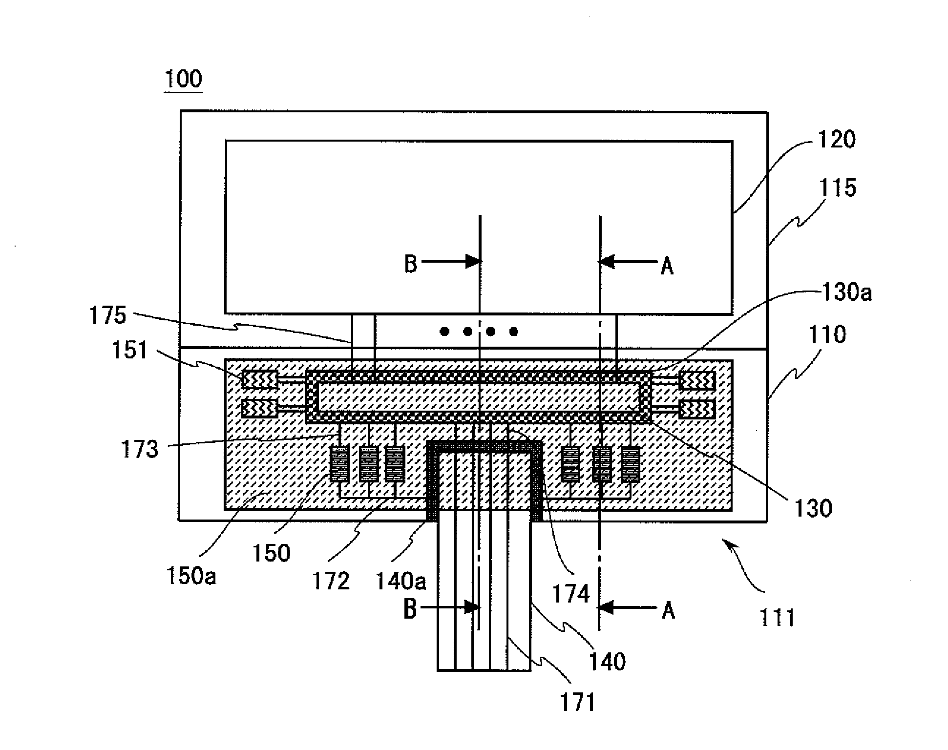
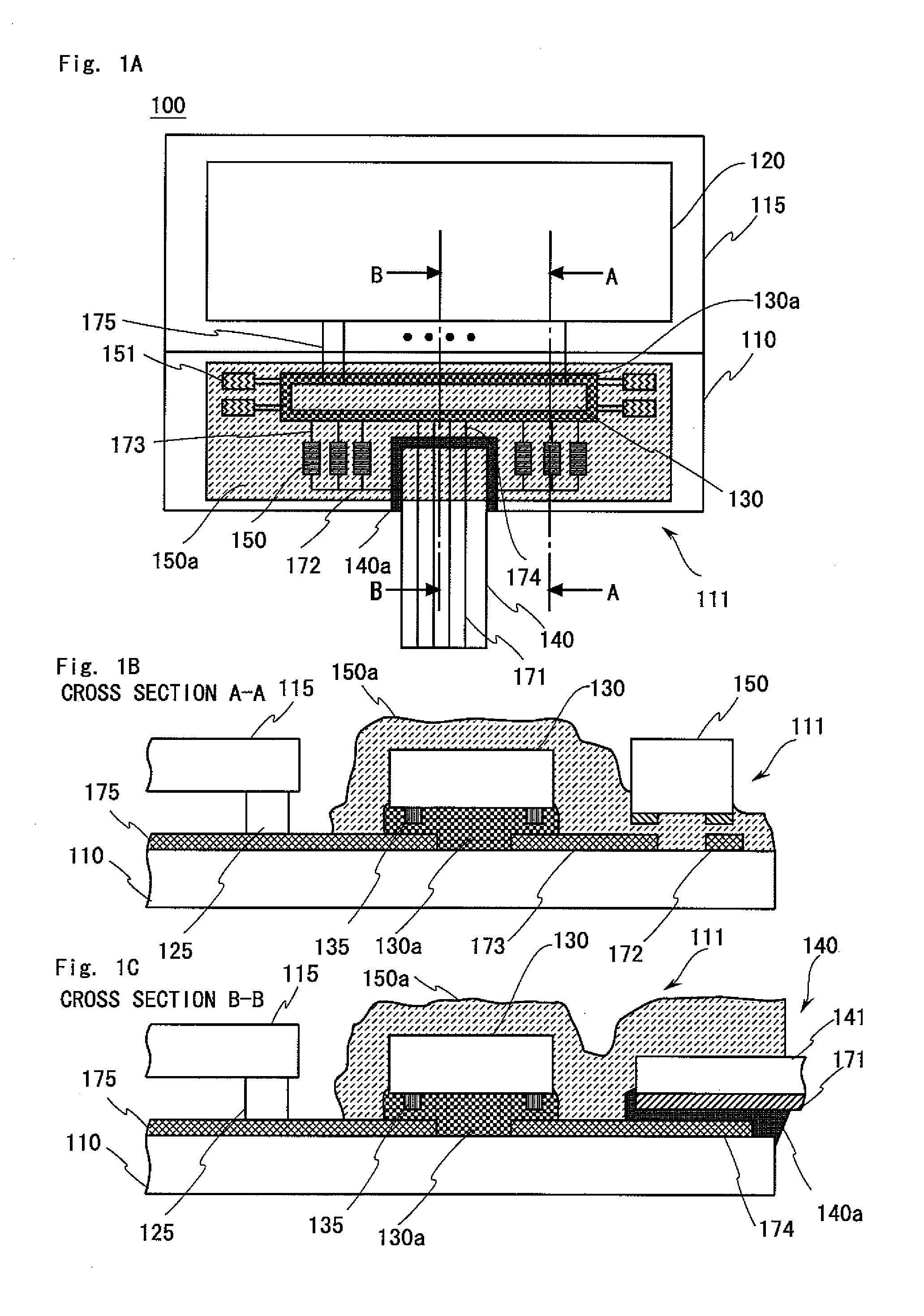
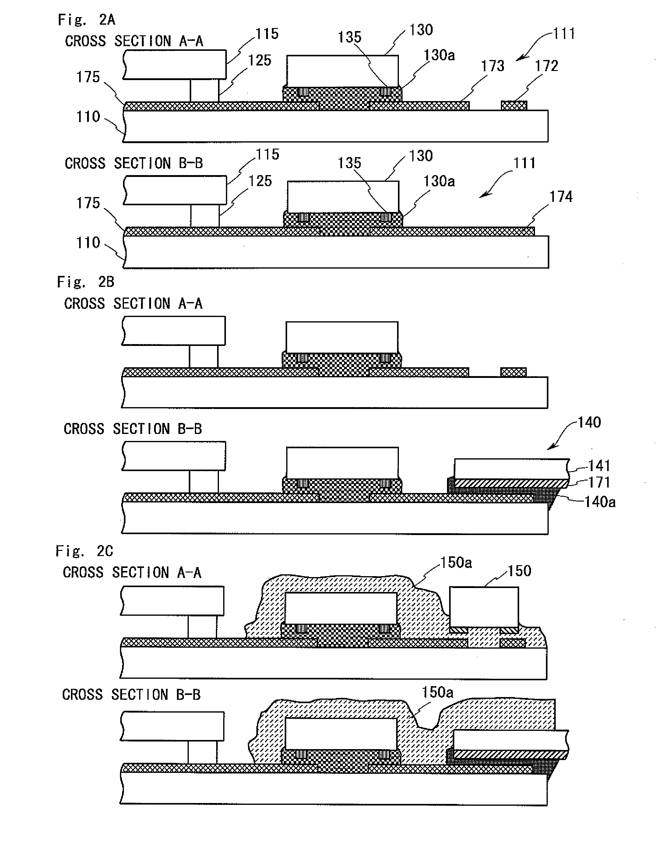
[0138]FIG. 1A is a schematic plan view showing a configuration of a liquid crystal display device 100 according to a first embodiment of the present invention, FIG. 1B is a cross-sectional view showing a cross section of the liquid crystal display device 100 taking along line A-A in FIG. 1A, and FIG. 1C is a cross-sectional view showing a cross section of the liquid crystal display device 100 taking along line B-B in FIG. 1A. As shown in FIGS. 1A to 1C, the liquid crystal display device 100 includes two glass substrates 110 and 115 disposed to face each other, an LSI chip 130, an FPC board 140, six stabilizing capacitors 150, and four boost capacitors 151.
[0139]A liquid crystal (not shown) is sealed in space sandwiched between the two glass substrates 110 and 115 by a sealing material 125, and a display portion 120 is formed on the glass substrate 115. On a projection 111 of the glass substrate 110 are moun...
second embodiment
3. Second Embodiment
[0158]3.1 Configuration of A Liquid Crystal Display Device
[0159]FIG. 3A is a schematic plan view showing a configuration of a liquid crystal display device 200 according to a second embodiment of the present invention, FIG. 3B is a cross-sectional view showing a cross section of the liquid crystal display device 200 taking along line C-C in FIG. 3A, and FIG. 3C is a cross-sectional view showing a cross section of the liquid crystal display device 200 taking along line D-D in FIG. 3A. As shown in FIGS. 3A to 3C, the liquid crystal display device 200 includes two glass substrates 110 and 115 disposed to face each other, an LSI chip 130, an FPC board 140, six stabilizing capacitors 150, and four boost capacitors 151. In the liquid crystal display device 200, the same or corresponding components as / to those of a liquid crystal display device 100 according to the first embodiment are denoted by the same reference numerals, and differences from the liquid crystal displ...
third embodiment
4. Third Embodiment
[0171]4.1 Configuration of A Liquid Crystal Display Device
[0172]FIG. 5A is a schematic plan view showing a configuration of a liquid crystal display device 300 according to a third embodiment of the present invention, FIG. 5B is a cross-sectional view showing a cross section of the liquid crystal display device 300 taking along line E-E in FIG. 5A, and FIG. 5C is a cross-sectional view showing a cross section of the liquid crystal display device 300 taking along line F-F in FIG. 5A. As shown in FIGS. 5A to 5C, the liquid crystal display device 300 includes two glass substrates 110 and 115 disposed to face each other, an LSI chip 130, an FPC board 140, six stabilizing capacitors 150, and four boost capacitors 151. In the liquid crystal display device 300, the same or corresponding components as / to those of a liquid crystal display device 100 according to the first embodiment are denoted by the same reference numerals, and differences from the liquid crystal display...
PUM
 Abstract
Description
Claims
Application Information