Fingerprint recognition module and electronic device comprising same

a fingerprint recognition module and fingerprint recognition technology, applied in the direction of instruments, non-linear optics, semiconductor/solid-state device details, etc., can solve the problems of increasing the thickness of the plurality of printed circuit boards, the inability of fingerprint recognition modules to be directly connected to the main board, and the limitation of the miniaturization of electronic devices, so as to reduce the size of the fingerprint recognition module and improve reliability, the effect of reducing the sub-section area

Active Publication Date: 2021-08-24
LG INNOTEK CO LTD
View PDF20 Cites 0 Cited by
  • Summary
  • Abstract
  • Description
  • Claims
  • Application Information

AI Technical Summary

Benefits of technology

[0022]According to the embodiment of the present invention, a flexible circuit board for chip on film having a two-layer structure is applied to a substrate of a fingerprint recognition module, and accordingly, a substrate area may be drastically reduced in response to a fine pitch. Moreover, the fine pitch may be implemented (Line / Space=10 μm or less / 15 μm or less) by using a polyimide substrate, thereby reducing a size of the fingerprint recognition module.
[0023]In addition, according to the embodiment of the present invention, different types of first chip, second chip, and third chip may be mounted on one substrate, thereby providing a fingerprint recognition module with improved reliability.
[0024]In addition, according to the embodiment of the present invention, a vibration space for a fingerprint sensor may be secured by forming an inner lead pattern portion on which the fingerprint sensor is mounted to have a height of 7 μm or more, and accordingly, the operational reliability of the fingerprint sensor may be improved.
[0025]In addition, according to the embodiment of the present invention, a fingerprint recognition module and a main board may be directly connected. Accordingly, a size and thickness of a flexible circuit board for transmitting a signal sensed by the fingerprint recognition module to the main board may be reduced. Moreover, it is possible to reduce a signal distance in which a signal formed by a fingerprint recognition chip is transmitted to the main board, thereby performing quickly fingerprint recognition.
[0026]Accordingly, a flexible circuit board for all-in-one chip on film according to the embodiment, a chip package including the same, and an electronic device including the same may increase spaces of other components and / or a battery space.
[0027]In addition, since connection of a plurality of printed circuit boards is not required, convenience of a process and reliability of electrical connection may be improved.

Problems solved by technology

However, such a fingerprint recognition module may not be directly connected to a main board.
An electronic device having a display unit requires a plurality of printed circuit boards, and thus there is a problem that a thickness is increased.
In addition, sizes of the plurality of printed circuit boards may be a limitation on miniaturization of the electronic device.
Further, poor bonding of the plurality of printed circuit boards may deteriorate reliability of the electronic device.

Method used


Image

  • Fingerprint recognition module and electronic device comprising same
  • Fingerprint recognition module and electronic device comprising same
  • Fingerprint recognition module and electronic device comprising same

Examples


Embodiment Construction

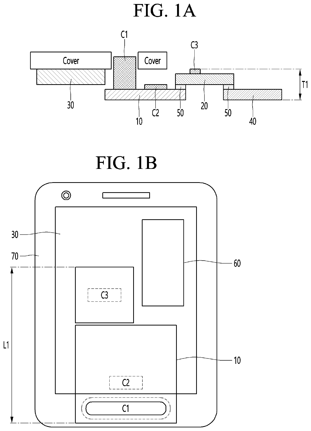
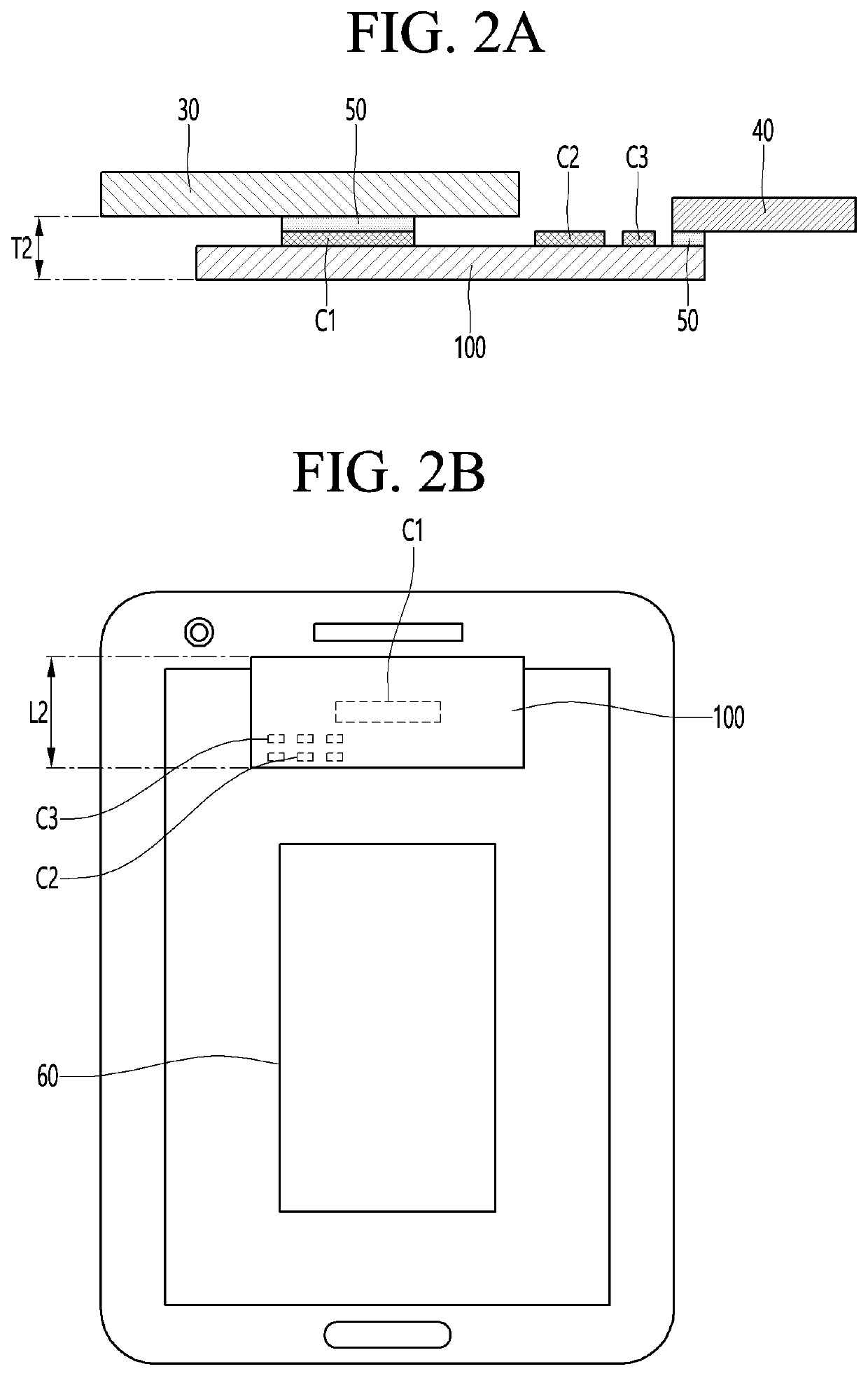
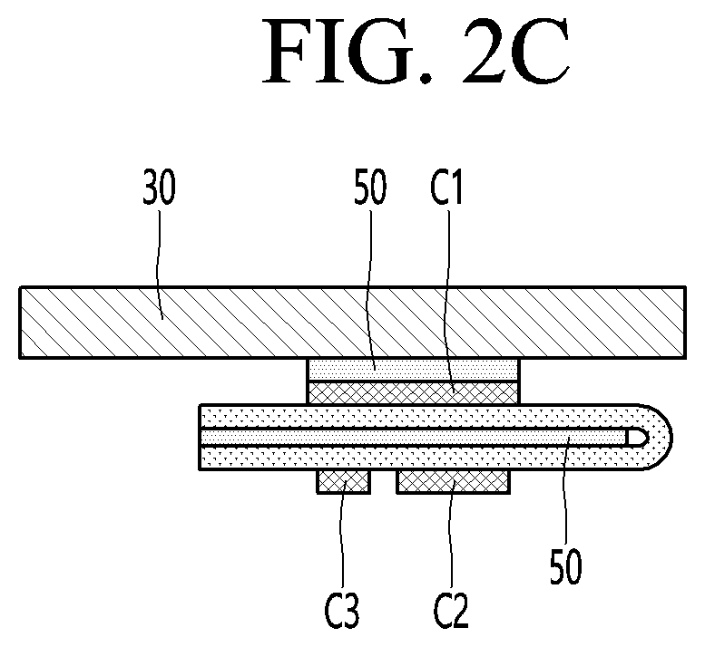
[0048]In the description of embodiments, when it is described that each layer (film), region, pattern, or structure is formed “above / on” or “below / under” a substrate, each layer (film), region, pad or pattern, the description includes being formed both “directly” or “indirectly (by interposing another layer)”“above / on” or “below / under”. A reference of above / on or below / under of each layer will be described with reference to the drawings

[0049]In addition, when a certain part is referred to as being “connected” to another part, it includes not only “directly connected” but also “indirectly connected” with another member therebetween. Further, when a certain part “includes” a certain component, unless described to the contrary, this means that other components may not be excluded, but other components may be further provided.

[0050]Hereinafter, embodiments of the present disclosure will be described in detail with reference to the accompanying drawings.

[0051]A printed circuit board acco...


PUM

PropertyMeasurementUnit
distanceaaaaaaaaaa
thicknessaaaaaaaaaa
distanceaaaaaaaaaa

Abstract

A fingerprint recognition module according to an embodiment comprises: a substrate; a conductive pattern portion disposed on the substrate; a protective layer partially disposed on one region of the conductive pattern portion; a first chip disposed on the conductive pattern portion exposed through a first open region of the protective layer; and a second chip disposed on the conductive pattern portion exposed through a second open region of the protective layer, wherein the first chip is a fingerprint recognition sensor, the second chip is an application specific integrated circuit, the substrate includes a first non-bending region located at one end thereof, a second non-bending region located at the other end opposite to the one end, and a bending region located between the first and the second non-bending region, the first open region is located on the first non-bending region, and the second open region is located on the second non-bending region.

Description

CROSS-REFERENCE TO RELATED PATENT APPLICATIONS[0001]This application is a U.S. National Stage Application under 35 U.S.C. § 371 of PCT Application No. PCT / KR2018 / 012699, filed Oct. 25, 2018, which claims priority to Korean Patent Application No. 10-2017-0178672, filed Dec. 22, 2017, whose entire disclosures are hereby incorporated by reference.TECHNICAL FIELD[0002]The present invention relates to a fingerprint recognition module, and more particularly, to a fingerprint recognition module having a bending structure and an electronic device including the fingerprint recognition module.BACKGROUND ART[0003]A fingerprint recognition sensor is a sensor for detecting fingerprints of a human finger, and is recently widely used as a means for enhancing security in portable electronic devices such as smartphones and tablet computers. That is, by performing a user registration or security authentication procedure through the fingerprint recognition sensor, the data stored in the portable elect...

Claims


Application Information

Patent Timeline
Patent Type & Authority Patents(United States)
IPC IPC(8): G06K9/20G06K9/00H01L27/32G02F1/1333H01L51/00
CPCG06K9/209G06K9/0002G02F1/13338H01L27/3234H01L27/3244H01L51/0097H01L2251/5338H01L23/28H01L23/48H01L2224/73204G02F1/136222H04M1/026H04M2250/12H04M1/0268Y02E10/549G06V40/1318H10K59/65H10K50/80H10K59/40H10K77/111H10K50/84G06V40/1306H10K59/12H10K2102/311
Inventor IM, SEONG HWANMIN, JUNG MYUNG
Owner LG INNOTEK CO LTD
Why Eureka
Try Eureka