Nickel-silicide formation with differential pt composition

Inactive Publication Date: 2011-07-14
AURIGA INNOVATIONS INC
View PDF9 Cites 11 Cited by
  • Summary
  • Abstract
  • Description
  • Claims
  • Application Information

AI Technical Summary

Benefits of technology

[0005]In view of the above concerns relating to the current process of NiSi formation, there remains a need for finding a solution that will enable NiSi formation with

Problems solved by technology

On the other hand, while being suitable as a contact material, NiSi is also known as a frequent cause of device defects which may be manifested by NiSi formed underneath masking spacer edges and particularly by NiSi formed in the direction of junction of a FET.
These defects, which are classified collectively as encroachment defects hereinafter, have been observed in almost every technology node since 65 nm node, may potentially cause device failure due to S/D-well and/or S/D-gate current leakage.
Unfortunately, the switch to using higher Pt content nickel-platinum alloy is also accompanied by a resistance penalty that is particularly less forgiving for technologies that integrate eDRAM, where strap

Method used


Image

  • Nickel-silicide formation with differential pt composition
  • Nickel-silicide formation with differential pt composition
  • Nickel-silicide formation with differential pt composition

Examples


Embodiment Construction

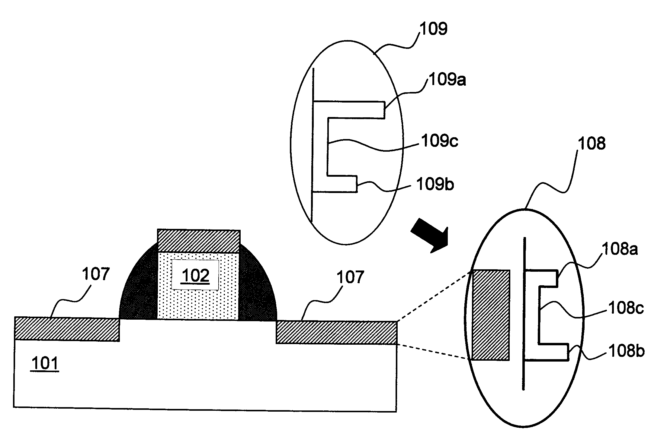
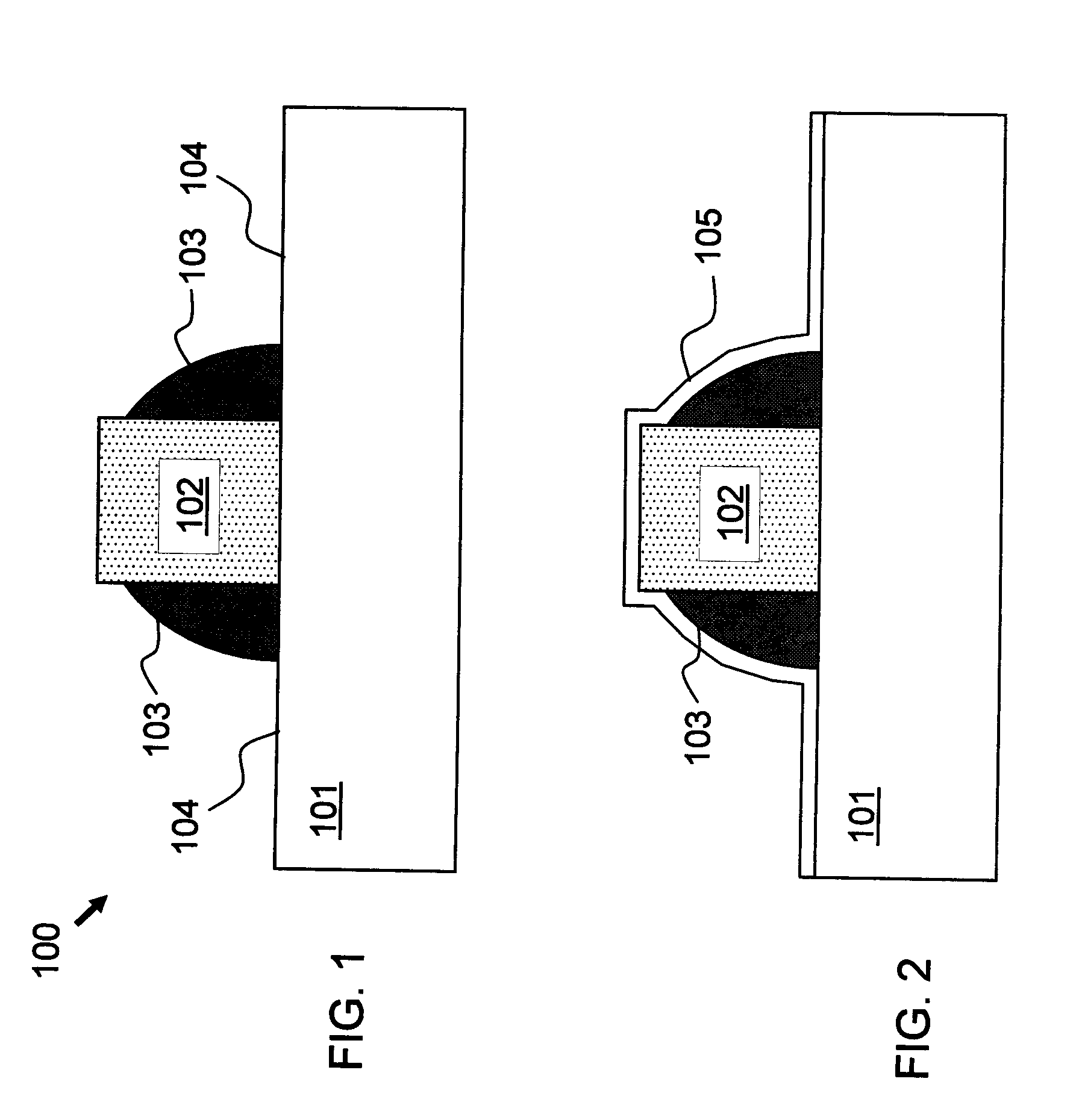
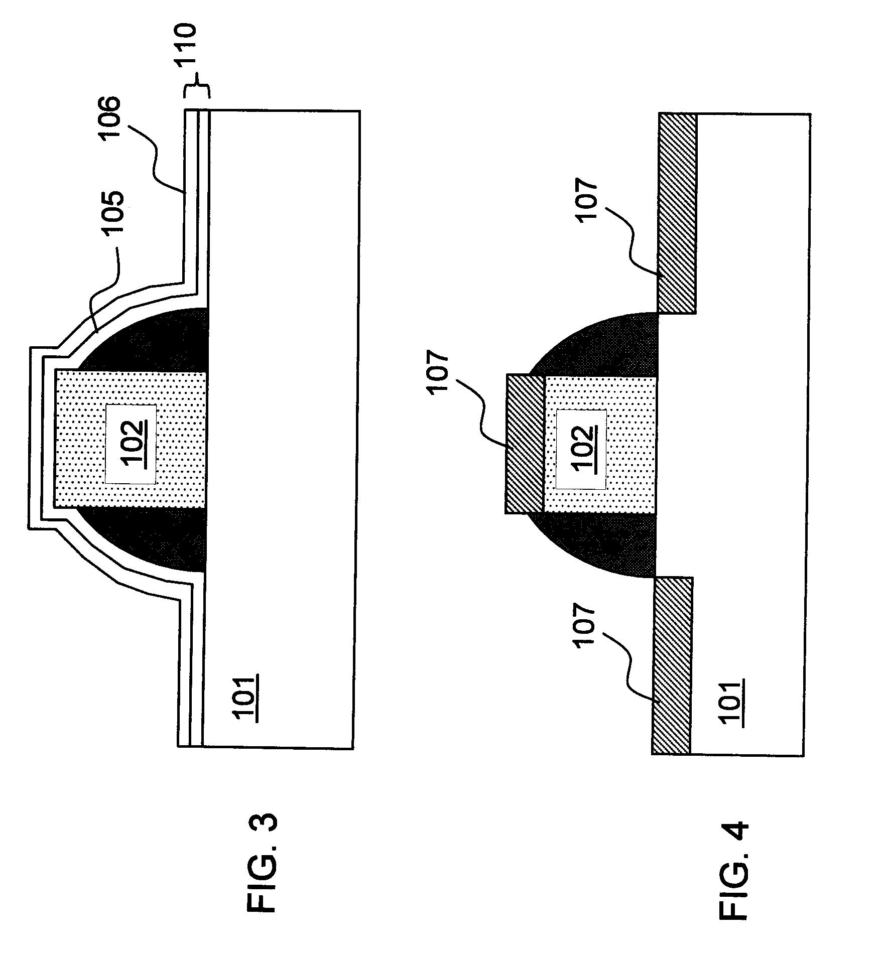
[0016]In the following detailed description, numerous specific details are set forth in order to provide a thorough understanding of various embodiments of the invention. However, it is to be understood that embodiments of the invention may be practiced without these specific details.

[0017]In the interest of not obscuring presentation of essences and / or embodiments of the invention, in the following detailed description, some processing steps and / or operations that are known in the art may have been combined together for presentation and / or for illustration purpose and in some instances may have not been described in detail. In other instances, some processing steps and / or operations that are known in the art may not be described at all. In addition, some well-known device processing techniques may have not been described in detail and, in some instances, may be referred to other published articles, patents, and / or patent applications for reference in order not to obscure descriptio...


PUM


Abstract

Embodiments of the invention provide a method of forming nickel-silicide. The method may include depositing first and second metal layers over at least one of a gate, a source, and a drain region of a field-effect-transistor (FET) through a physical vapor deposition (PVD) process, wherein the first metal layer is deposited using a first nickel target material containing platinum (Pt), and the second metal layer is deposited on top of the first metal layer using a second nickel target material containing no or less platinum than that in the first nickel target material; and annealing the first and second metal layers covering the FET to form a platinum-containing nickel-silicide layer at a top surface of the gate, source, and drain regions.

Description

FIELD OF THE INVENTION[0001]The present invention relates generally to the field of semiconductor device manufacturing and in particular relates to method of forming nickel-silicide with differential platinum composition.BACKGROUND OF THE INVENTION[0002]Nickel-silicide (NiSi) is an important and frequently used contact material for semiconductor devices such as field-effect-transistors (FETs), which are usually applied in the source (S), drain (D), and / or gate (G) regions of a FET. On the other hand, while being suitable as a contact material, NiSi is also known as a frequent cause of device defects which may be manifested by NiSi formed underneath masking spacer edges and particularly by NiSi formed in the direction of junction of a FET. These defects, which are classified collectively as encroachment defects hereinafter, have been observed in almost every technology node since 65 nm node, may potentially cause device failure due to S / D-well and / or S / D-gate current leakage. Therefo...

Claims


Application Information

Patent Timeline
IPC IPC(8): H01L29/78H01L21/3205
CPCH01L29/665H01L21/28518
Inventor FRYE, ASASIMON, ANDREW
Owner AURIGA INNOVATIONS INC
Why Eureka
Try Eureka