Light emitting element and manufacturing method thereof

a technology manufacturing methods, which is applied in the direction of lasers, semiconductor devices, semiconductor lasers, etc., can solve the problems of increasing threshold current, enlarge the piezoelectric field, and increase the strain, so as to improve the yield of light emitting elements, reduce the diffusion of oxygen, and superior the effect of reactivity

Inactive Publication Date: 2011-04-19
SHARP FUKUYAMA LASER CO LTD
View PDF8 Cites 0 Cited by
  • Summary
  • Abstract
  • Description
  • Claims
  • Application Information

AI Technical Summary

Benefits of technology

[0010]In view of the foregoing, it is an object of the present invention to provide nitride semiconductor laser elements in which the resonator facets are protected with a view to improved yields.
[0013]According to the present invention, as the first facet through which light is emitted, the N-pole plane of a nitride semiconductor is used. Since the N-pole plane is superior in reactivity compared with another plane, forming the first protective film on this plane allows reaction at the interface to provide firm joint. This makes it possible to reduce diffusion of oxygen over the interface, and to secure wide process windows for the first and second protection films. It is thus possible to improve the yields of the light emitting elements.

Problems solved by technology

Increasing the In content, however, increases the strain due to lattice mismatch between GaN and InGaN, and thus enlarges the piezoelectric field.
This results in problems of increased threshold current and lower light emission efficiency.
Moreover, since a nitride semiconductor having a wurzite structure, a hexagonal crystal structure, has no symmetric planes with respect to the c axis direction, polarities appear in a nitride semiconductor grown in the c axis direction, and thus spontaneous polarization occurs, another factor leading to the problems.
However, it is difficult to form a nitride semiconductor layered structure on the m or a plane of a substrate as compared with forming it on the c plane, resulting in a problem of lower yields.
Since a nitride semiconductor laser element emits light with a short wavelength and high energy, its resonator facets are prone to be damaged, another factor leading to lower yields.
In nitride semiconductors in particular, oxidation of facets may greatly affect the occurrence of COD.

Method used


Image

  • Light emitting element and manufacturing method thereof
  • Light emitting element and manufacturing method thereof
  • Light emitting element and manufacturing method thereof

Examples


Embodiment Construction

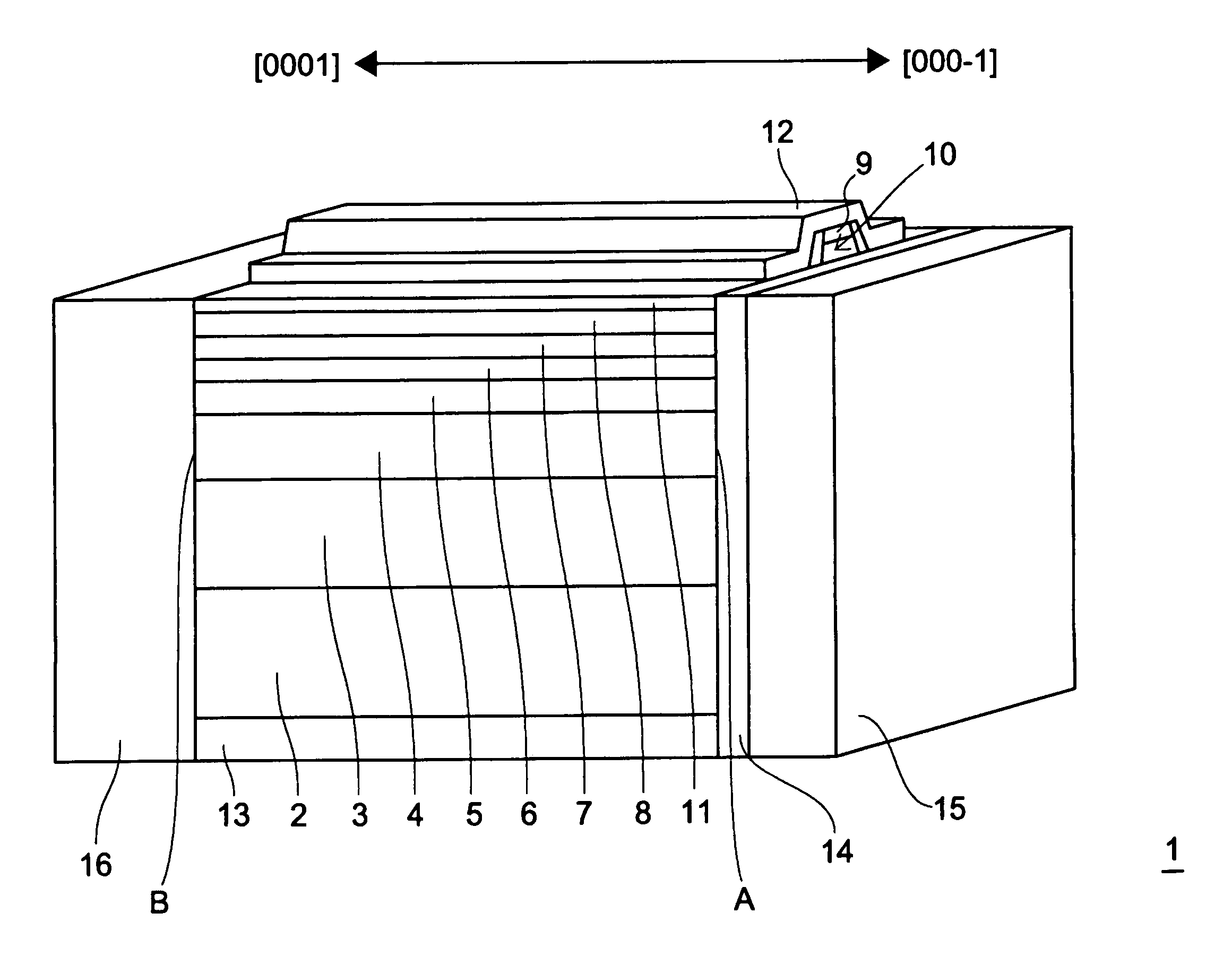
GaN Crystal Structure

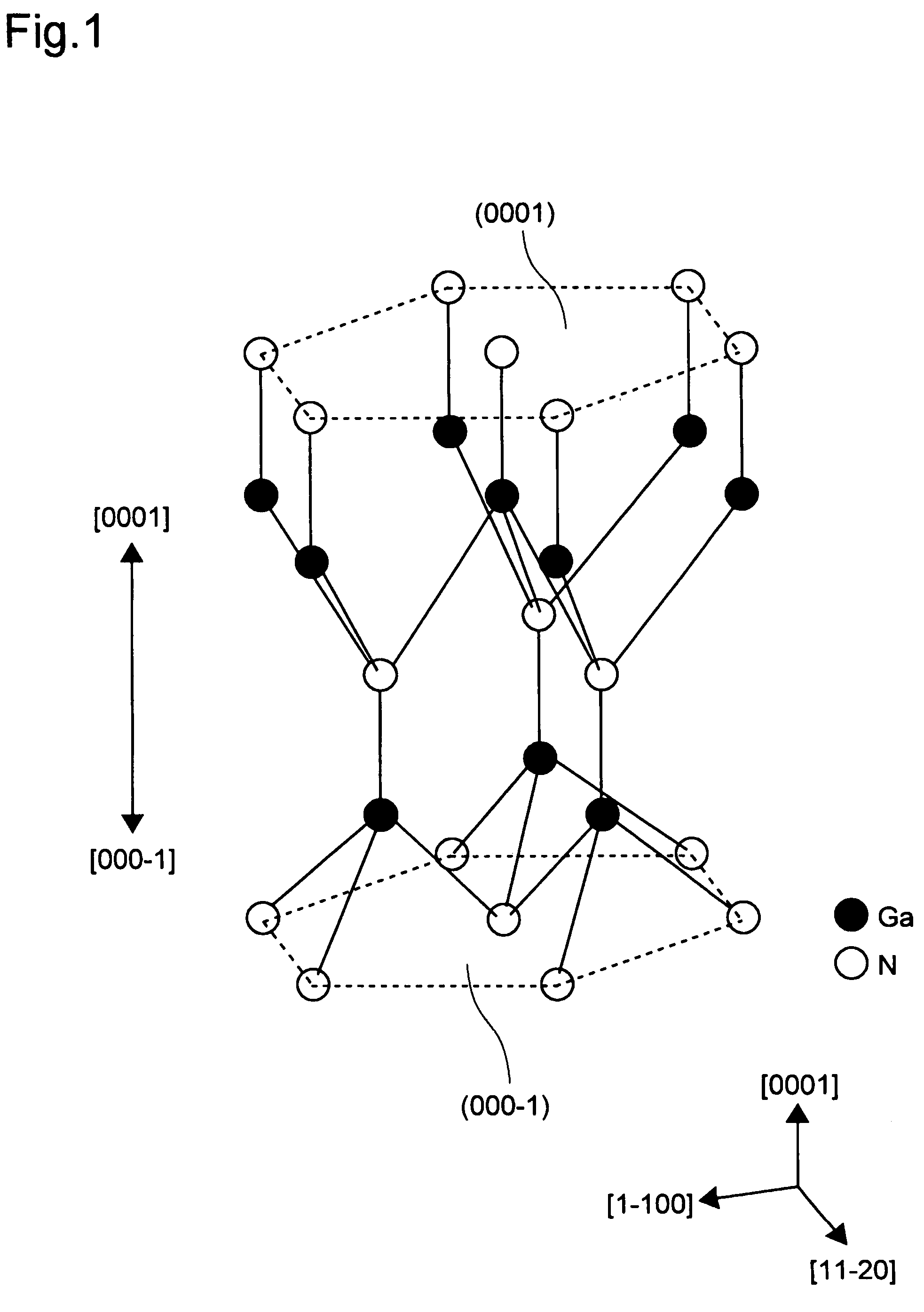
[0018]First, with reference to FIG. 1, a wurzite-type crystal structure will be described with GaN given as an example. FIG. 1 is a schematic view of a crystal structure of GaN, in which a black dot represents a Ga atom, and a white dot represents an N atom.

[0019]As shown in FIG. 1, the Ga atoms and the N atoms each have one bond parallel to the c axis and three bonds extending to the side opposite from that one bond and not parallel to the c axis. For each of the Ga atoms, the one bond that is parallel to the c axis extends to the [0001] side whereas the three bonds that are not parallel to the c axis extend to the [000-1] side. As opposed to this, for each of the N atoms, the one bond that is parallel to the c axis extends to the [000-1] side whereas the three bonds that are not parallel to the c axis extend to the [0001] side.

[0020]As described above, there are no symmetrical facets in the c axis direction in the GaN crystal structure. Accordingly, this cryst...


PUM


Abstract

In a laser chip 1 using a nitride semiconductor having a hexagonal crystal structure, the −c plane is used as a first resonator facet A, which is the side of the laser chip 1 through which light is emitted. On the first resonator facet A, that is, on the −c plane, a facet protection film 14 is formed. This ensures firm joint between the first resonator facet A and the facet protection film 14 and alleviates deterioration of the first resonator facet A.

Description

[0001]This application is based on Japanese Patent Application No. 2007-316006 filed on Dec. 6, 2007, the contents of which are hereby incorporated by reference.BACKGROUND OF THE INVENTION[0002]1. Field of the Invention[0003]The present invention relates to light emitting elements and a manufacturing method thereof. More particularly, the present invention relates to light emitting elements as exemplified by laser elements using nitride semiconductors, and to a manufacturing method thereof.[0004]2. Description of Related Art[0005]Being compounds between a group-III element, such as Al, Ga or In, and N, a group-V element, nitride-based semiconductors (for example, AlN, GaN and InN, including solid solutions of these, such as AlGaN and InGaN-in the present specification all these are collectively called nitride semiconductors) are, for their band structure and chemical stability, expected to find applications as materials for light emitting elements and power devices.[0006]On the othe...

Claims


Application Information

Patent Timeline
Patent Type & Authority Patents(United States)
IPC IPC(8): H01L33/10H01L33/16H01S5/028H01S5/22H01S5/343
CPCB82Y20/00H01S5/028H01S5/34333H01S5/0282H01S5/2201H01S5/0281
Inventor KAWAKAMI, TOSHIYUKIKAWAGUCHI, YOSHINOBUKAMIKAWA, TAKESHI
Owner SHARP FUKUYAMA LASER CO LTD
Why Eureka
Try Eureka