Apparatus and Method for Improving Photoresist Properties Using a Quasi-Neutral Beam

Inactive Publication Date: 2011-07-21
TOKYO ELECTRON LTD
View PDF14 Cites 39 Cited by
  • Summary
  • Abstract
  • Description
  • Claims
  • Application Information

AI Technical Summary

Benefits of technology

[0014]The invention can provide apparatus and methods of processing a substrate in real-time using subsystems and processing sequences created to cure and/or harden radiation-sensitive materials. In addition, the hardened radi

Problems solved by technology

However, the use of plasma (i.e., electrically charged particles), itself, produces problems in the manufacture of semiconductor devices.
Therefore, the tolerance of semiconductor structures for the charge carried by particles impinging on them during the manufacturing process, such as a dry plasma etching process, has become quite limited and the structures for

Method used


Image

  • Apparatus and Method for Improving Photoresist Properties Using a Quasi-Neutral Beam
  • Apparatus and Method for Improving Photoresist Properties Using a Quasi-Neutral Beam
  • Apparatus and Method for Improving Photoresist Properties Using a Quasi-Neutral Beam

Examples


Embodiment Construction

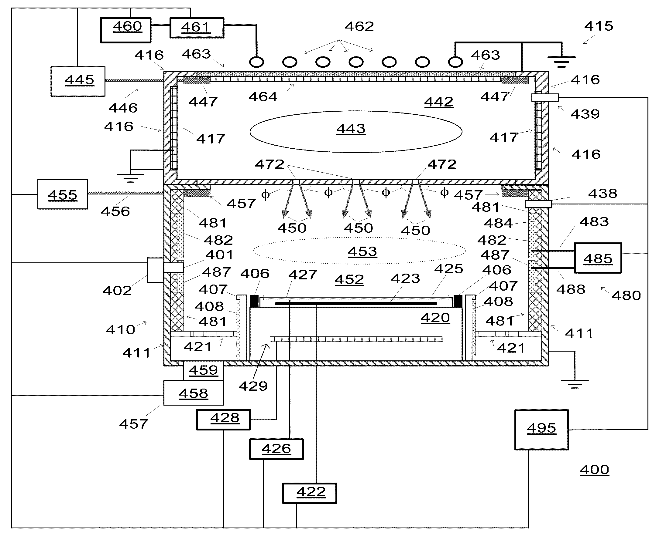
[0025]The invention provides apparatus and methods of processing a substrate in real-time using subsystems and processing sequences created to cure and / or harden radiation-sensitive materials. In addition, the cured and / or hardened radiation-sensitive material layer can be used to more accurately control gate and / or spacer critical dimensions (CDs), to control gate and / or spacer CD uniformity, and to eliminate and / or reduce line edge roughness (LER) and line width roughness (LWR).

[0026]In some embodiments, apparatus and methods are provided for creating and / or using a metrology library that includes profile data and diffraction signal data for cured and / or hardened radiation-sensitive material (photoresist) features and periodic structures.

[0027]One or more evaluation features can be provided at various locations on a substrate and can be used to evaluate and / or verify Q-NB curing (hardening) procedures and associated models. Substrates can have real-time and historical data associa...


PUM

PropertyMeasurementUnit
Temperatureaaaaaaaaaa
Pressureaaaaaaaaaa

Abstract

The invention can provide apparatus and methods of processing a substrate in real-time using a Quasi-Neutral Beam (Q-NB) curing system to improve the etch resistance of photoresist layer. In addition, the improved photoresist layer can be used to more accurately control gate and/or spacer critical dimensions (CDs), to control gate and/or spacer CD uniformity, and to eliminate line edge roughness (LER) and line width roughness (LWR).

Description

BACKGROUND OF THE INVENTION[0001]1. Field of the Invention[0002]The present invention relates to substrate processing, and more particularly to improving the substrate processing using radiation-sensitive material (photoresist) curing and / or hardening procedures, and subsystems.[0003]2. Description of the Related Art[0004]During semiconductor processing, plasma is often utilized to assist etch processes by facilitating the anisotropic removal of material along fine lines or within vias (or contacts) patterned on a semiconductor substrate. Furthermore, plasma is utilized to enhance the deposition of thin films by providing improved mobility of adatoms on a semiconductor substrate.[0005]Once the plasma is formed, selected surfaces of the substrate are etched by the plasma. The process is adjusted to achieve appropriate conditions, including an appropriate concentration of desirable reactant and ion populations to etch various features (e.g., trenches, vias, contacts, etc.) in the sele...

Claims


Application Information

Patent Timeline
IPC IPC(8): B01J19/08
CPCH01J37/32009H01J37/3233H01J37/32357H01J37/32422H01J2237/338H01J37/32449H01J37/32458H01J37/32532H01J37/3244
Inventor FUNK, MERRITTCHEN, LEESUNDARARAJAN, RADHA
Owner TOKYO ELECTRON LTD
Why Eureka
Try Eureka