
Semiconductor device

Active Publication Date: 2011-07-21
SEMICON ENERGY LAB CO LTD
View PDF99 Cites 94 Cited by
  • Summary
  • Abstract
  • Description
  • Claims
  • Application Information

AI Technical Summary

Benefits of technology

[0013]Note that all of the transistors included in the storage circuit do not need to be provided with oxide semiconductors. It is preferable to provide a place where high-speed operation is required with a transistor including a semiconductor material other than an oxide semiconductor. Examples of such a semiconductor material include single crystal silicon.

Problems solved by technology

In the case where a storage circuit is formed with the use of these two kinds of transistor in combination, the storage circuit is unsuitable to increase the storage capacity per unit area when the two transistors are juxtaposed.

Method used


Image

  • Semiconductor device
  • Semiconductor device
  • Semiconductor device

Examples


Embodiment Construction

[0046]Examples of an embodiment of the present invention will be described below with reference to the drawings. Note that the present invention is not limited to the following description, and it will be easily understood by those skilled in the art that various changes and modifications can be made without departing from the spirit and scope of the present invention. Therefore, the present invention should not be construed as being limited to the following description of the embodiments.

[0047]Note that the position, size, range, and the like of each component illustrated in the drawings which are referred in the following description are not actual ones in some cases to make them simple and make features stand out. Therefore, the present invention is not limited to the position, size, range, and the like disclosed in the drawings.

[0048]Note that in the following description, ordinal numbers such as “first”, “second”, and “third” are used for convenience in order to avoid confusion...


PUM


Abstract

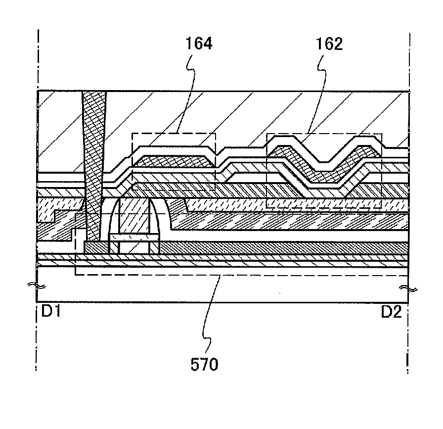
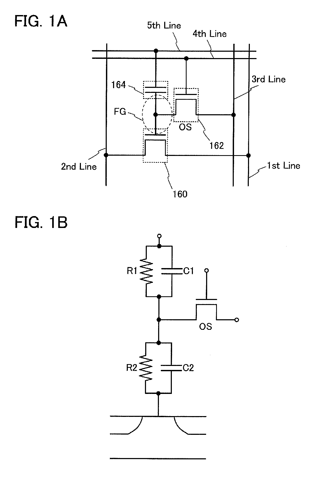
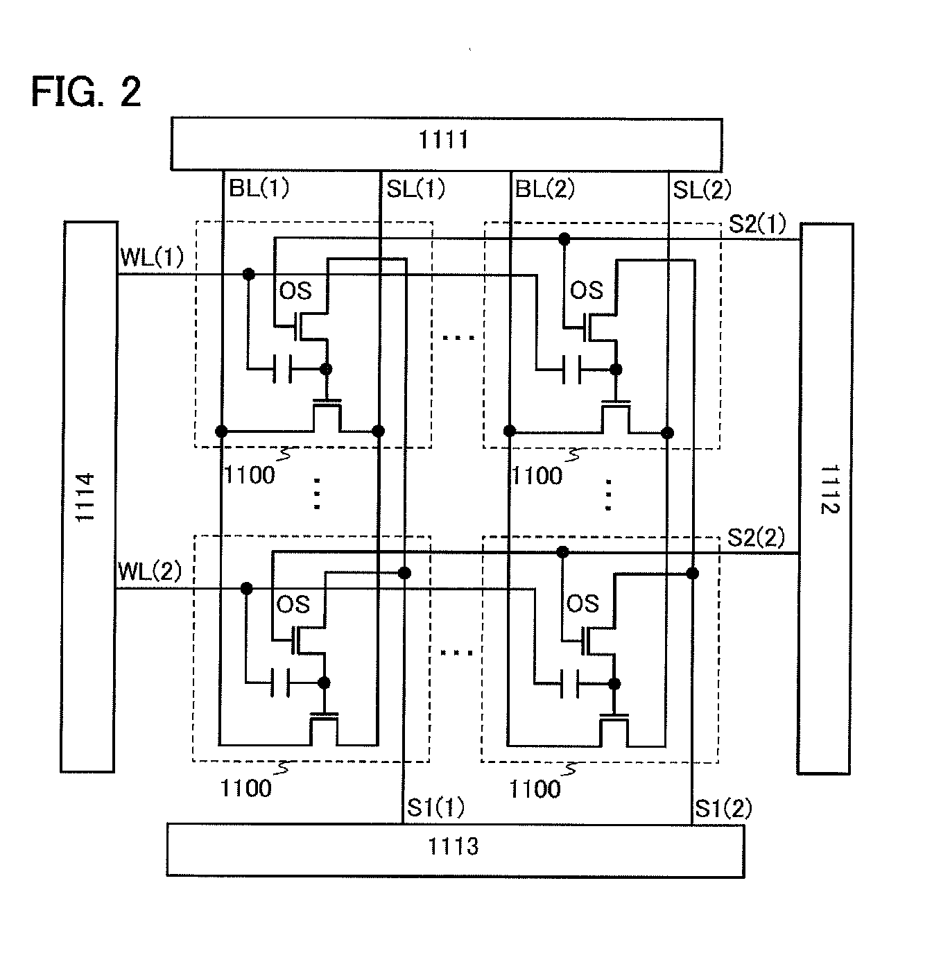
To provide a storage device in which advantages of both a nonvolatile storage device and a volatile storage device can be obtained, a semiconductor device includes a first transistor provided in or over a substrate and a second transistor provided above the first transistor, where at least part of the first transistor and the second transistor are overlapped with each other, and a gate electrode of the first transistor and a source or drain electrode of the second transistor are electrically connected to each other. It is preferable that the first transistor be provided using single crystal silicon and the second transistor be provided using an oxide semiconductor having extremely low off-state current.

Description

TECHNICAL FIELD[0001]An embodiment of the present invention relates to a semiconductor device and a manufacturing method thereof, in particular, a semiconductor device capable of storing data.[0002]A semiconductor device refers to a device provided with at least one semiconductor element such as a transistor. Thus, a storage device is included in the semiconductor device. Note that the storage device refers to a device which includes a plurality of storage elements.BACKGROUND ART[0003]Storage devices using semiconductor elements are broadly classified into two categories: a volatile storage device that loses stored data when power supply stops, and a nonvolatile storage device that holds stored data even when power is not supplied.[0004]Examples of a volatile storage device include a dynamic random access memory (hereinafter referred to as a DRAM) and a static random access memory (hereinafter referred to as an SRAM).[0005]When a DRAM is formed using a conventional transistor, a dat...

Claims


Application Information

Patent Timeline
IPC IPC(8): H01L27/088H01L27/108
CPCH01L21/8221H01L27/0688H01L27/105H01L27/1052H01L27/1207H01L27/1225H01L27/1156H01L2924/00011H10B41/70H01L2224/80001H01L27/1255H10B99/00
Inventor YAMAZAKI, SHUNPEIKOYAMA, JUNKATO, KIYOSHI
Owner SEMICON ENERGY LAB CO LTD
Learn More