Semiconductor integrated circuit and operating voltage control method
- Summary
- Abstract
- Description
- Claims
- Application Information
AI Technical Summary
Benefits of technology
Problems solved by technology
Method used
Image

Examples
first embodiment
1. First Embodiment
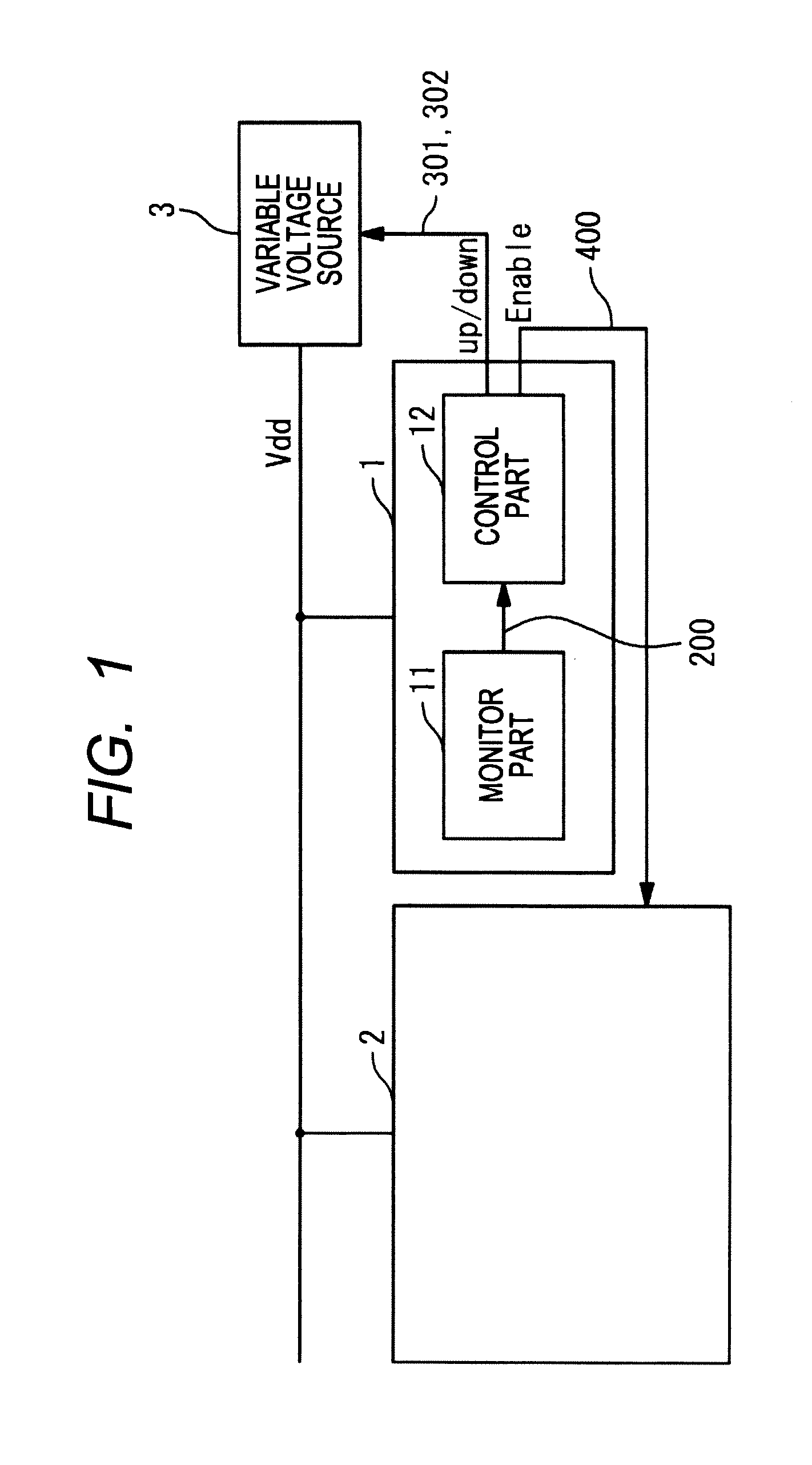
[0041]The semiconductor integrated circuit according to a first embodiment of the present invention will be described with FIGS. 1 to 9. FIG. 1 is a diagram illustrating one example of the configuration of a semiconductor integrated circuit according to the present invention. Referring to FIG. 1, the semiconductor integrated circuit according to the present invention includes a circuit part 1 designed under a first corner condition, a circuit part 2 designed under a second corner condition, and a variable voltage source 3.
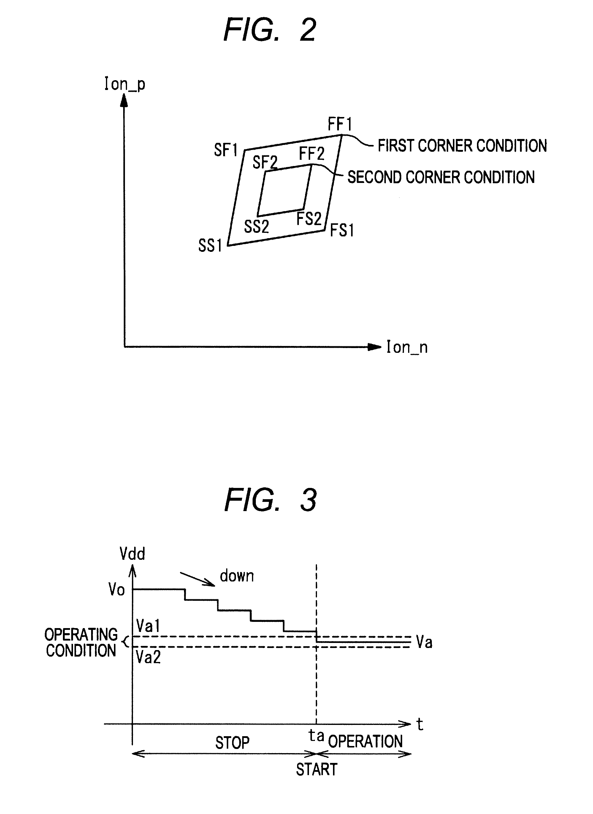
[0042]FIG. 2 is a graph showing an example of the corner conditions according to the present invention. The circuit parts 1 and 2 are circuit blocks each having a complementary metal oxide semiconductor (CMOS). Referring to FIG. 2, it is assumed that an on-state current Ion_P of a p-channel MOS transistor in the CMOS is on the Y-axis, an on-state current Ion_N of an n-channel MOS transistor is on the X-axis. It is also assumed that a current valu...
second embodiment
2. Second Embodiment
[0106]A semiconductor integrated circuit according to a second embodiment of the present invention will be described with reference to FIGS. 1 and 11 to 14. The semiconductor integrated circuit according to the second embodiment includes the circuit part 1 designed under the first corner condition, the circuit part 2 designed under the second corner condition, and the variable voltage source 3, as in the first embodiment illustrated in FIG. 1. The semiconductor integrated circuit according to the second embodiment is different in only the monitor part 11 and the control part 12, and other configurations are identical with those in the first embodiment, and therefore their detailed description will be omitted.
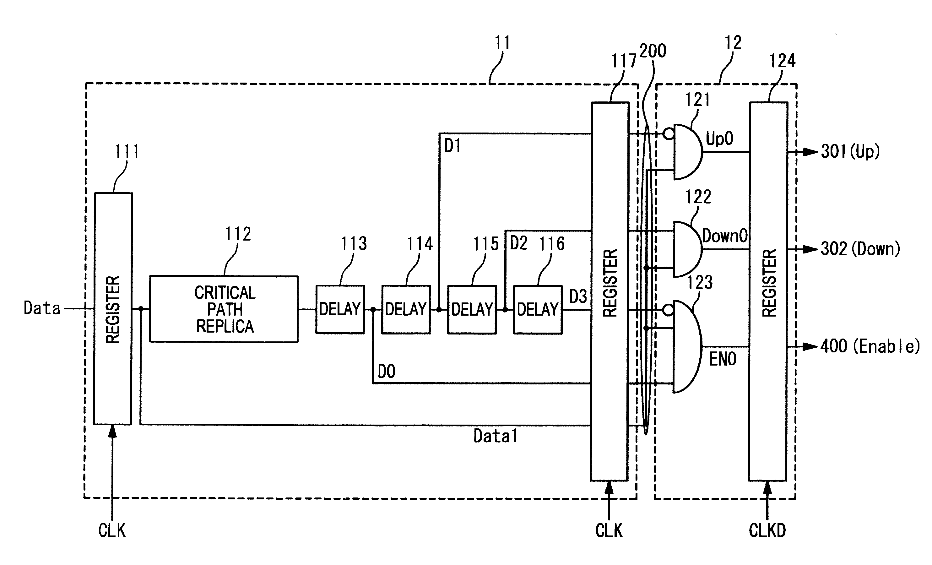
[0107]The monitor part 11 according to the second embodiment includes a ring oscillator having a clock signal as the monitor output 200. The control part 12 counts the number of oscillations of the monitor output 200 in a given period, and determines the sign...
third embodiment
3. Third Embodiment
[0121]As described in the first and second embodiments, control is made so that the circuit part 2 stops even during the operation of the semiconductor integrated circuit. During this period, when the control signal is input from a CPU or another control part which are not shown to the circuit part 2, there is a risk that there is no response, and an error occurs. For that reason, as illustrated in FIG. 15, it is preferred to further include an emulator 4 that operates during the stop of the circuit part 2 and a selector 5 in addition to the semiconductor integrated circuit of the first and second embodiments.
[0122]Referring to FIG. 15, the circuit part 2 and the emulator 4 receive a control signal 500 from a CPU or another control part not shown. The circuit part 2 operates to output a signal responsive to the control signal 500 to the selector 5. The emulator 4 is realized by, for example, a small-scaled low-speed processor designed under the first corner condit...
PUM
 Abstract
Description
Claims
Application Information
 - Generate Ideas
- Intellectual Property
- Life Sciences
- Materials
- Tech Scout
- Unparalleled Data Quality
- Higher Quality Content
- 60% Fewer Hallucinations
Browse by: Latest US Patents, China's latest patents, Technical Efficacy Thesaurus, Application Domain, Technology Topic, Popular Technical Reports.
© 2025 PatSnap. All rights reserved.Legal|Privacy policy|Modern Slavery Act Transparency Statement|Sitemap|About US| Contact US: help@patsnap.com