Conductive structure for high gain antenna and antenna

a high gain antenna and conductive structure technology, applied in the direction of antennas, antenna feed intermediates, basic electric elements, etc., can solve the problems of increasing the energy loss of the antenna feed proportionally to the number of antennas, the structure of the antenna becomes complicated, and the efficiency of the antenna deteriorates, so as to improve the efficiency, improve the efficiency of the antenna, and improve the directivity of the antenna

Inactive Publication Date: 2011-07-21
ELECTRONICS & TELECOMM RES INST
View PDF8 Cites 11 Cited by
  • Summary
  • Abstract
  • Description
  • Claims
  • Application Information

AI Technical Summary

Benefits of technology

[0007]As described below, the conductive structure according to the present invention can be readily produced by using low cost PCB technology. In addition, due to the conductive upper structure of the antenna using the conductive structure according to the present invention, efficiency, gain, and directivity of the antenna can be enhanced by using a simple source. A feeding structure is more simplified than the case where a related arrangement antenna technique is used, and loss of antenna supply power can be prevented. Furthermore, the gain of the antenna can be increased regardless of a resonance distance between the ground plane of the antenna and the conductive structure disposed above the antenna such that the spatial volume of the antenna can be reduced.

Problems solved by technology

However, in arrangement antennas having such a shape, as the number of antennas arranged increases, an energy loss due to antenna feeding increases proportionally to the number of antennas used for feeding.
As such, the efficiency of an antenna deteriorates, and the structure of the antenna becomes complicated due to fine adjustment of a feeding length, etc. to obtain a proper gain and radiation patterns.

Method used


Image

  • Conductive structure for high gain antenna and antenna
  • Conductive structure for high gain antenna and antenna
  • Conductive structure for high gain antenna and antenna

Examples


Embodiment Construction

[0021]The present invention will now be described more fully with reference to the accompanying drawings, in which exemplary embodiments of the invention are shown.

[0022]The invention may, however, be embodied in many different forms and should not be construed as being limited to the embodiments set forth herein; rather, these embodiments are provided so that this disclosure will be thorough and complete, and will fully convey the concept of the invention to those of ordinary skill in the art.

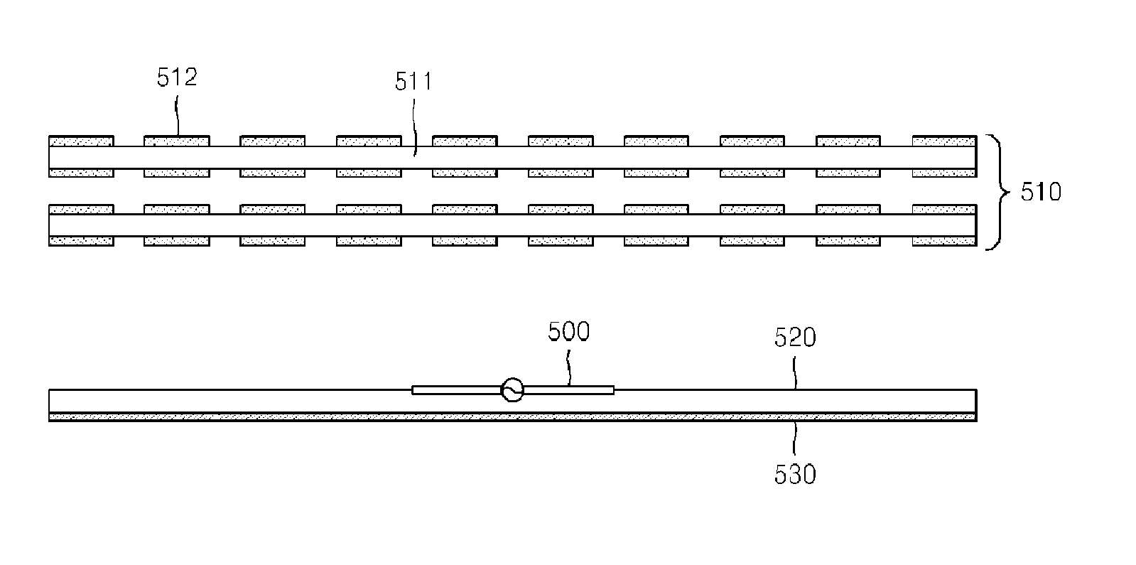
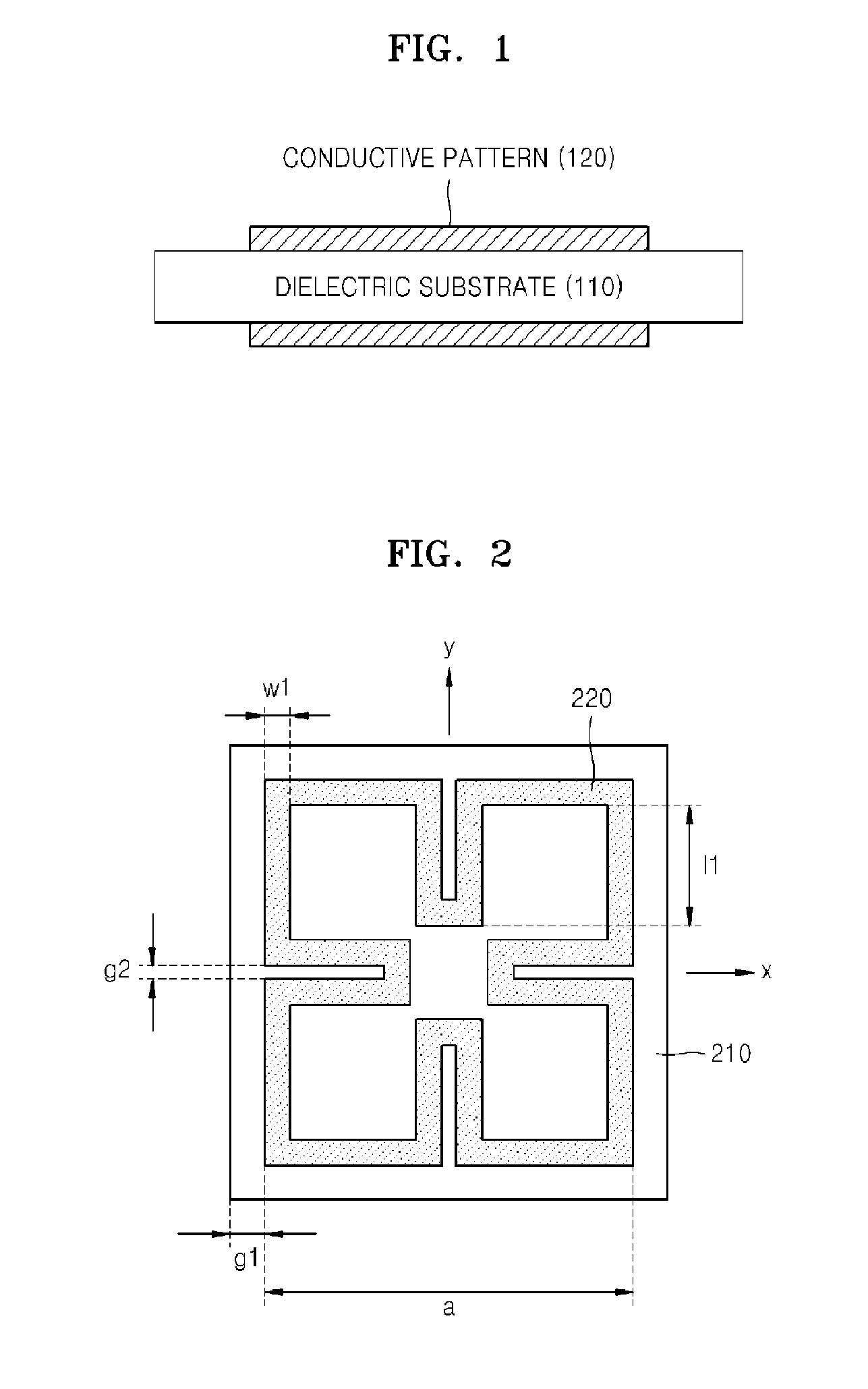
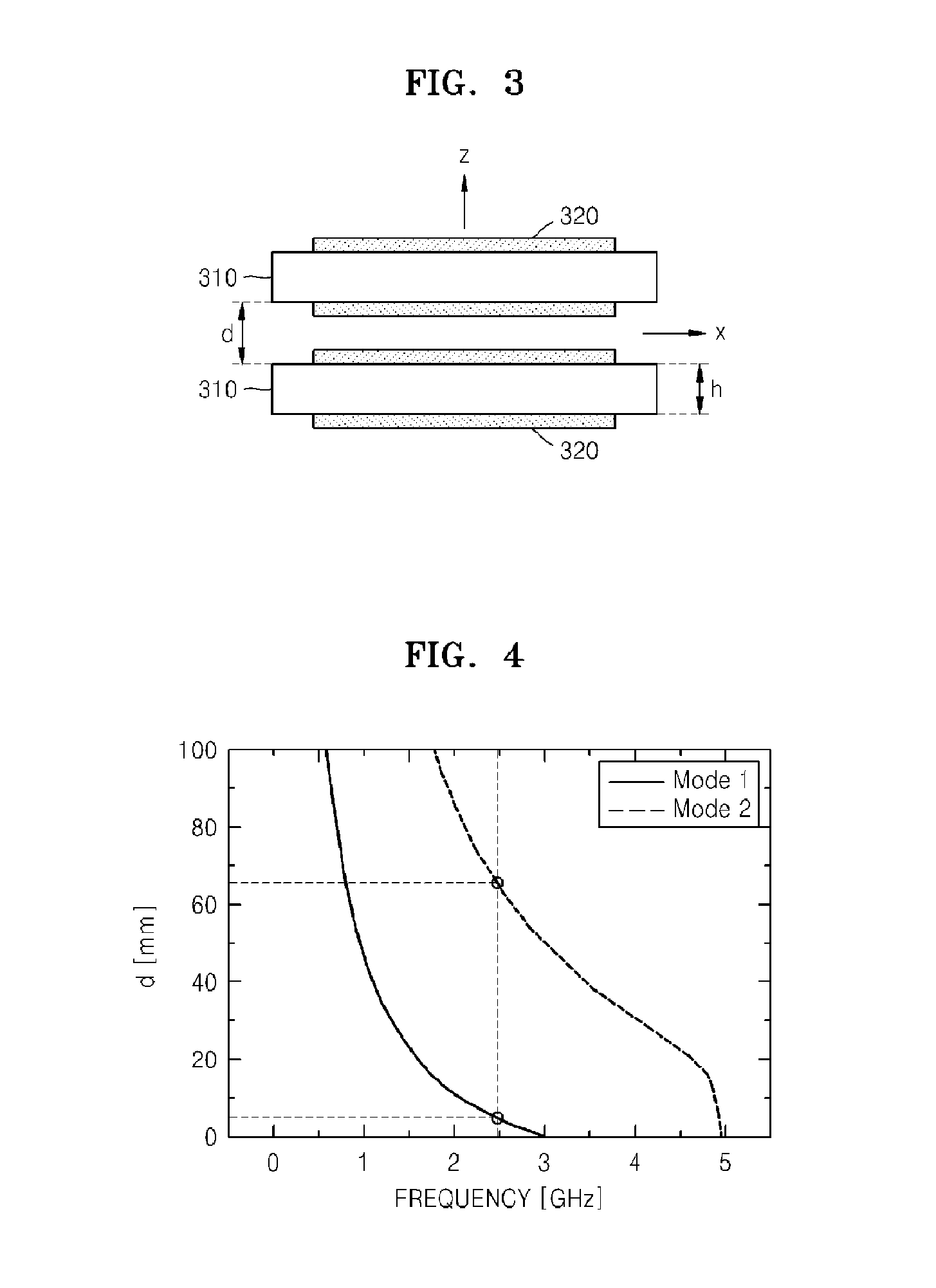
[0023]FIG. 1 illustrates the construction of a conductive structure according to an embodiment of the present invention.

[0024]Referring to FIG. 1, the conductive structure according to the current embodiment includes a dielectric substrate 110 and a plurality of conductive patterns 120. The dielectric substrate 110 is formed of a general dielectric material, and the conductive patterns 120 are etched on top and bottom surfaces of the dielectric substrate 110. The conductive structure can be re...


PUM


Abstract

Provided are a conductive structure for a high gain antenna and an antenna. A plurality of conductive patterns (512) of the conductive structure are formed on top and bottom surfaces of a dielectric substrate (511) positioned above the antenna and separated from an antenna body (500). A conductive upper structure of the antenna (510) is positioned above the antenna opposite to a ground plane (530) to which the antenna body is fed, separated from the antenna body. A conductive unit structure comprising a plurality of conductive patterns (512) formed on top and bottom surfaces of the dielectric substrate (511) is arranged in a plurality of layers. The conductive structure for a high gain antenna and the antenna can be readily produced by using low cost printed circuit board (PCB) technology, and a gain of the antenna can be increased regardless of a resonance distance between the ground plane of the antenna and the conductive structure disposed above the antenna.

Description

TECHNICAL FIELD[0001]The present invention relates to a conductive structure for a high gain antenna and an antenna, and more particularly, to an antenna having a conductive structure attached to an upper portion of the antenna including a ground plane, in which a plurality of conductive patterns having particular discretionary shapes and intervals are formed on top and bottom surfaces of a dielectric substrate by using low-priced printed circuit board (PCB) technology, and the conductive structure in the antenna.BACKGROUND ART[0002]In the related art, arrangement antennas in which a plurality of patch antennas are arranged above an antenna, are used in a place where a high gain radiation characteristic is needed, such as in a base station, so as to increase a gain of a base station antenna.[0003]However, in arrangement antennas having such a shape, as the number of antennas arranged increases, an energy loss due to antenna feeding increases proportionally to the number of antennas ...

Claims


Application Information

Patent Timeline
Patent Type & Authority Applications(United States)
IPC IPC(8): H01Q19/06
CPCH01Q1/38H01Q21/062H01Q9/26H01Q13/08
Inventor JU, JEONGHOCHOI, JAE-ICKLEE, WANGJOOKIM, DONGHO
Owner ELECTRONICS & TELECOMM RES INST
Why Eureka
Try Eureka