Method for driving display device and liquid crystal display device

a display device and liquid crystal technology, applied in the direction of digital storage, instruments, computing, etc., can solve the problems of reducing the voltage applied to a liquid crystal element, affecting the display quality, so as to reduce the degradation of display quality and reduce power consumption at the time of displaying still images.

Active Publication Date: 2011-07-21
SEMICON ENERGY LAB CO LTD
View PDF50 Cites 118 Cited by
  • Summary
  • Abstract
  • Description
  • Claims
  • Application Information

AI Technical Summary

Benefits of technology

[0010]In view of the above problems, an object of an embodiment of the present invention is to reduce power consumption without a complicated operation in a driver circuit of a display device. Another object of an embodiment of the present invention is to reduce degradation in the display quality.
[0016]With an embodiment of the present invention, power consumption at the time of displaying a still image can be reduced. In addition, degradation in the display quality can be reduced.

Problems solved by technology

However, in the above-mentioned driving methods, a structure and operation of a driver circuit which supplies a signal to a scan line or a signal line of the liquid crystal display device are complicated, so that power consumption of the liquid crystal display device cannot be reduced enough.
Further, in the case where the break period during which no scan line and no signal line are selected is provided as in Patent Document 1, the interval between writing operations into pixels becomes long, which may cause the voltage applied to a liquid crystal element be largely decreased due to leakage current of a transistor or parasitic capacitance in some cases.
Large decrease in the voltage applied to the liquid crystal element degrades the display quality; for example, display with a predetermined gray scale level cannot be performed.
Further in the above liquid crystal display devices, the luminance changes due to its own temperature change, and even in the case of displaying a still image, the change in luminance gradually becomes larger as the time passes, thereby degrading the display quality.

Method used


Image

  • Method for driving display device and liquid crystal display device
  • Method for driving display device and liquid crystal display device
  • Method for driving display device and liquid crystal display device

Examples


embodiment 1

[0034]In this embodiment, a liquid crystal display device in which the timing to start or stop operation of a driver circuit is controlled in accordance with the ambient temperature will be described as an example of a display device.

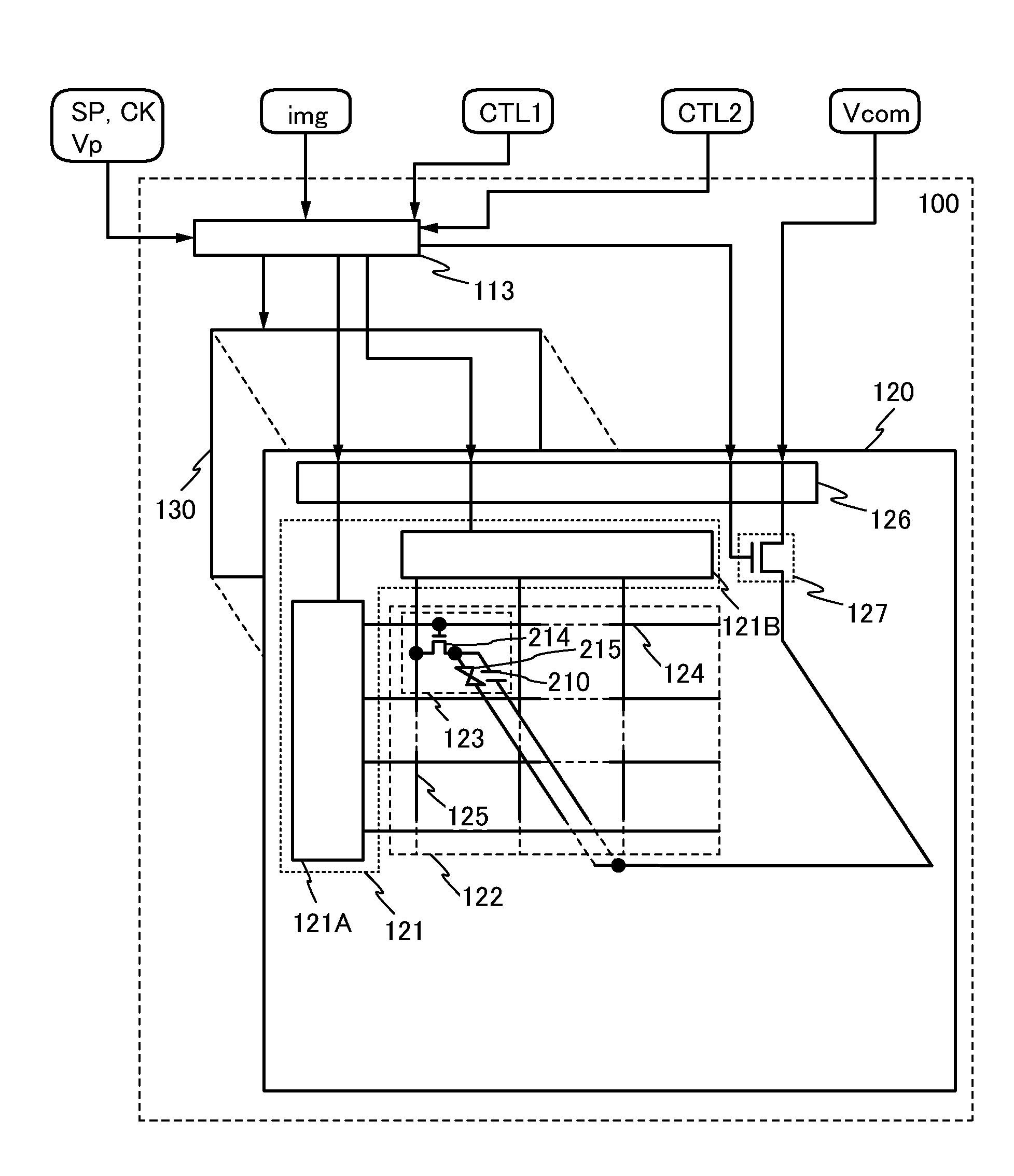
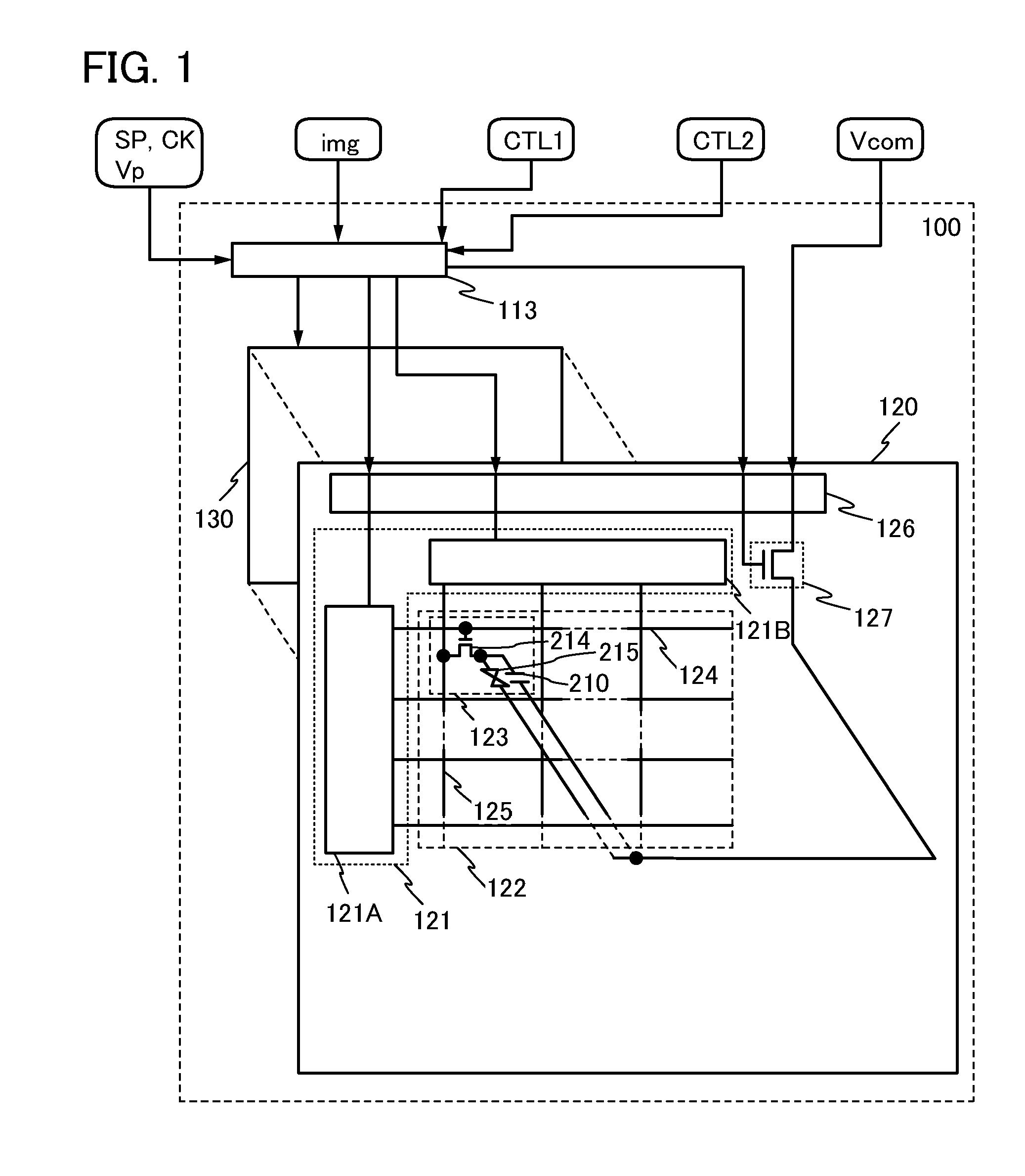
[0035]First, an example of the structure of the liquid crystal display device of this embodiment will be described with reference to FIG. 1. FIG. 1 is a block diagram illustrating an example of the structure of a liquid crystal display device.

[0036]A liquid crystal display device 100 illustrated in FIG. 1 includes a display control circuit 113 in which output of a signal or voltage is controlled on the basis of a control signal CTL1 and a control signal CTL2, and a display panel 120 whose display operation is controlled by the display control circuit 113.

[0037]Note that the term “voltage” generally means a difference between potentials at two points (also referred to as a potential difference). However, in some cases, values of both a voltage and a pote...

embodiment 2

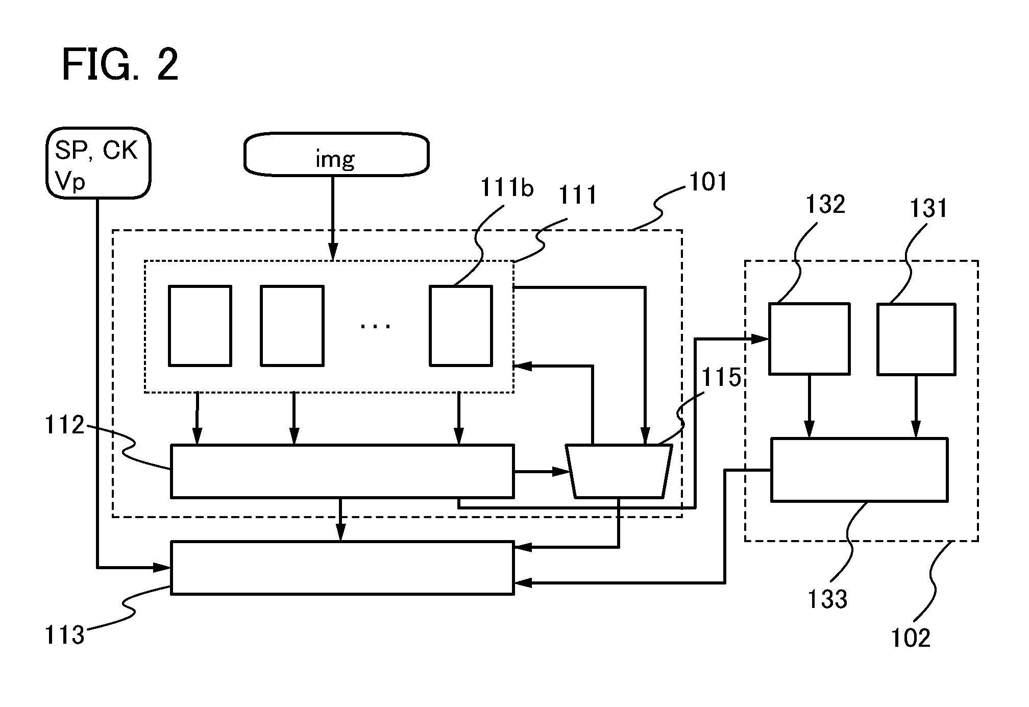
[0138]In this embodiment, an example of a shift register which can be used in a scan line driver circuit and a signal line driver circuit of the display device described in the above embodiment will be described.

[0139]An example of the structure of the shift register in this embodiment will be described with reference to FIGS. 8A to 8C. FIGS. 8A to 8C are diagrams illustrating an example of the structure of the shift register of this embodiment.

[0140]The shift register illustrated in FIG. 8A includes a first to N-th pulse output circuits 10—1 to 10_N (N is a natural number greater than or equal to 3).

[0141]Each of the first to N-th pulse output circuits 10—1 to 10_N includes a first input terminal 21, a second input terminal 22, a third input terminal 23, a fourth input terminal 24, a fifth input terminal 25, a first output terminal 26, and a second output terminal 27 (see FIG. 8B). The first input terminal 21, the second input terminal 22, and the third input terminal 23 of each on...

embodiment 3

[0170]In this embodiment, a transistor which can be used in the display device of the above embodiment will be described.

[0171]As the structure of the transistor which can be used in the display device of the above embodiment, a top-gate structure, a bottom-gate structure, and the like can be given, for example. Further, a staggered structure or a planar structure can be employed as the bottom-gate structure, for example.

[0172]The transistor described in the above embodiment may have a structure in which one channel formation region is formed (also referred to as a single-gate structure) or a structure in which a plurality of channel formation regions is formed (also referred to as a multi-gate structure). Alternatively, the transistor which can be used in the display device of the above embodiment may have a structure in which two gate electrode layers are provided over and below a channel formation region each with a gate insulating layer interposed therebetween (also referred to ...


PUM


Abstract

The still image display mode includes a first period of writing the data of the image signal from the driver circuit portion into the pixel; after the first period, a second period of stopping supply of a signal or voltage for operating the driver circuit portion to the driver circuit portion; and after the second period, a third period of restarting the supply of a signal or voltage for operating the driver circuit portion to the driver circuit portion and writing the data of the image signal into the pixel from the driver circuit portion, so that the pixel keeps displaying a still image. A length of a period from the stop of the supply of the signal for operating the driver circuit portion to the driver circuit portion to the restart is set in accordance with a temperature of the display device.

Description

TECHNICAL FIELD[0001]An embodiment of the present invention relates to a method for driving a display device. Another embodiment of the present invention relates to a liquid crystal display device.BACKGROUND ART[0002]Display devices such as liquid crystal display devices have been applied in a wide range of fields from large-sized display devices such as TV sets to small-sized display devices such as mobile phones, and those with higher added value have been developed. In recent years, in view of improvement in convenience of mobile devices for example, development of display devices with low power consumption has attracted attention.[0003]For example, Patent Document 1 discloses a technique for reducing the power consumption of a liquid crystal display device, in which all signal lines are electrically disconnected from a signal line driver circuit and a high impedance state is formed in order to keep the voltage of each signal line constant in a break period during which no scan l...

Claims


Application Information

Patent Timeline
Patent Type & Authority Applications(United States)
IPC IPC(8): G06F3/038
CPCG09G3/3655G09G2320/041G09G2320/103G09G3/36G09G2340/0435G11C19/28G09G2330/021
Inventor HAYAKAWA, MASAHIKOWAKIMOTO, KENICHI
Owner SEMICON ENERGY LAB CO LTD
Why Eureka
Try Eureka