Display device

Inactive Publication Date: 2011-08-04
CHUNGHWA PICTURE TUBES LTD
View PDF7 Cites 3 Cited by
  • Summary
  • Abstract
  • Description
  • Claims
  • Application Information

AI Technical Summary

Benefits of technology

An objective of the present invention is to provide a display device of which parasitic capacitances can be reduced.
Another objective of the present invention is to provide a display device of which the stability of displaying images is increased.
In the present invention, the conducting material located above an electrical conductive structure that is disposed on the side of a TFT array substrate facing a CF substrate is removed, and an empty area is thereby formed in the dummy region. The electrical conductive structure has no conducting material residing above, and thus parasitic capacitances are reduced. Moreover, the transmission of electronic signals on the electrical conductive structure becomes more stable, and thereby increasing the stability of displaying images.

Problems solved by technology

The parasitic capacitances may affect the stability of displaying images.

Method used


Image

  • Display device
  • Display device
  • Display device

Examples


first embodiment

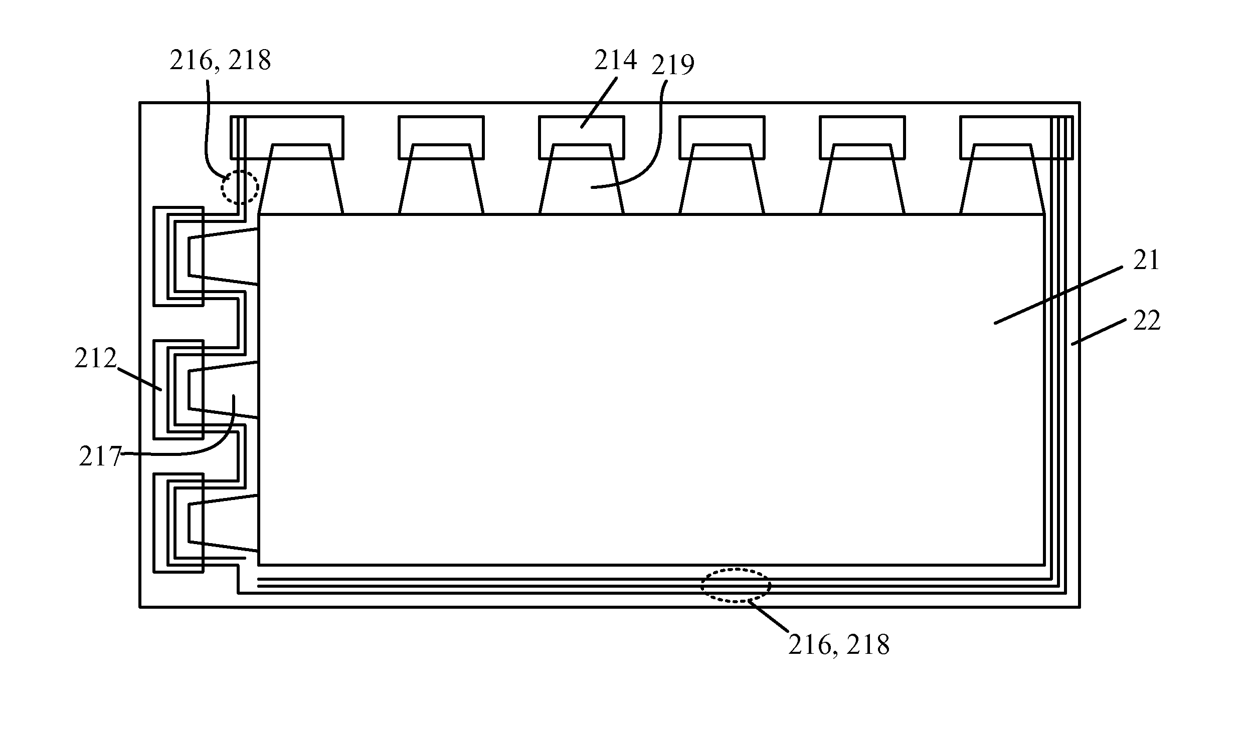
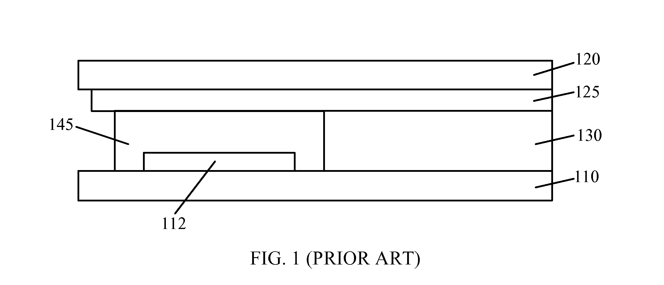
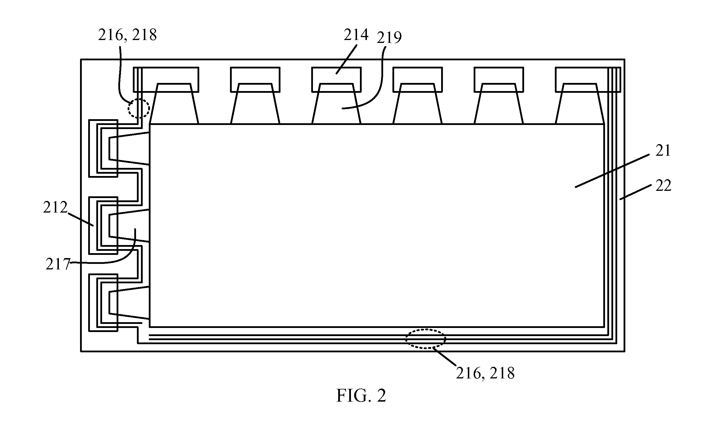
FIG. 3A and FIG. 3B are diagrams showing cross-sectional views of liquid crystal display devices implemented according to the present invention. It is noted that FIG. 3A and FIG. 3B only show the structures respectively corresponding to the gate driver circuit 212 and source driver circuit 214 of the dummy region 22 in FIG. 2 instead of showing the whole structures of the LCD devices. As shown in FIG. 3A and FIG. 3B, the LCD device includes a thin-film transistor (TFT) array substrate 210, a color filter (CF) substrate 220, and a liquid crystal layer 230. The two substrates 210, 220 are facing each other, and the liquid crystal layer 230 is disposed therebetween. A transparent conducting layer 225 is disposed on the side of the CF substrate 220 facing the TFT array substrate 210. The transparent conducting layer 225 is disposed over both the active region 21 and the dummy region 22, and serves as a common electrode of the display panel for providing a fixed voltage. The transparent ...

second embodiment

FIG. 4A, FIG. 4B and FIG. 4C are diagrams showing cross-sectional views of liquid crystal display devices implemented according to the present invention. It is noted that FIG. 4A, FIG. 4B and FIG. 4C only show the structures corresponding to the repair line 216 and signal lines 218 of the dummy region 22 in FIG. 2, instead of showing the whole structures of the LCD devices.

As shown in FIG. 2 and FIG. 4A, the repair line 216 of the dummy region 22 is disposed on the side of the TFT array substrate 210 facing the CF substrate 220. The repair line 216 is facing or opposite to an empty area 2252 of the transparent conducting layer 225. The empty area 2252 is formed by removing a conducting material of the transparent conducting layer 225. Since the conducting material located above the repair line 216 is removed, the repair line 216 has no conducting material residing above, and parasitic capacitances are thereby reduced.

In another aspect, the conducting material of the transparent cond...

third embodiment

FIG. 5A and FIG. 5B are diagrams showing cross-sectional views of liquid crystal display devices implemented according to the present invention. It is noted that FIG. 5A and FIG. 5B only show the structures corresponding to the gate wires 217 or source wires 219 of the dummy region 22 in FIG. 2 instead of showing the whole structures of the LCD devices.

As shown in FIG. 2 and FIG. 5A, the gate wires 217 which is utilized for connecting the scan lines (not shown) to the gate driver circuit 212 and the source wires 219 which is utilized for connecting the data lines (not shown) to the source driver circuit 214 are disposed on the side of the TFT array substrate 210 facing the CF substrate 220. The gate wires 217 (or the source wires 219) are facing or opposite to an empty area 2255 of the transparent conducting layer 225. The empty area 2255 is formed by removing a conducting material of the transparent conducting layer 225. Since the conducting material located above the gate wires 21...


PUM


Abstract

A display device has a display panel that is divided into an active region for displaying images and a dummy region outside of the active region. The display device comprises a first substrate and a second substrate disposed in parallel and spaced apart from each other; a plurality of electrical conductive structures disposed on the first substrate and located within the dummy region; and a transparent conducting layer disposed on the second substrate and disposed over both the active region and the dummy region, the transparent conducting layer being utilized for providing a fixed voltage, wherein the transparent conducting layer in the dummy region has an empty area facing at least one electrical conductive structure. The empty area is formed by removing a conducting material of the transparent conducting layer. Parasitic capacitances in display device can be reduced.

Description

TECHNICAL FIELD OF THE INVENTIONThe present invention relates to a display device, and more particularly, to a display device having a patterned transparent conductive layer.BACKGROUND OF THE INVENTIONNowadays, how to reduce the manufacturing cost of a display device is an important topic. As gate-in-panel (GIP) technological skills have been matured, that a gate driver circuit is directly implemented on a display panel has become an efficient way to reduce the cost of the display device.Please refer to FIG. 1, which is a diagram showing a cross-sectional view of a conventional liquid crystal display (LCD) device utilizing the gate-in-panel technique. As shown in FIG. 1, the conventional LCD device includes a thin-film transistor (TFT) array substrate 110, a color filter (CF) substrate 120, and a liquid crystal layer 130. The two substrates 110, 120 are facing each other, and the liquid crystal layer 130 is disposed therebetween. A transparent conducting layer 125 is disposed on the...

Claims


Application Information

Patent Timeline
IPC IPC(8): G02F1/1333G02F1/1343
CPCG02F1/1343G02F1/1333G02F1/136204G02F1/133388G02F1/1345G02F1/13452G09G2300/0426G02F1/1309G02F1/136259
Inventor SHIH, MEI-SHA
Owner CHUNGHWA PICTURE TUBES LTD
Why Eureka
Try Eureka