Eureka AIR delivers breakthrough ideas for toughest innovation challenges, trusted by R&D personnel around the world.

Current limiting circuit

Inactive Publication Date: 2011-08-11
RENESAS ELECTRONICS CORP
View PDF7 Cites 11 Cited by
  • Summary
  • Abstract
  • Description
  • Claims
  • Application Information

AI Technical Summary

Benefits of technology

[0019]The circuit configuration as described above enables accurate control of the current flowing through the output transistor even when a temperature change occurs.
[0020]According to an exemplary aspect of the present invention, it is possible to provide a current limiting circuit capable of accurately controlling a current flowing through an output transistor even when a temperature change occurs.

Problems solved by technology

As a result, excessive power may be applied to the power supply semiconductor.
Thus, Japanese Unexamined Patent Application Publication No. 2008-236528 has a problem in that when the resistance component of the wire 217 varies due to a temperature change, a current flowing through the output transistor 201 cannot be accurately controlled.
This causes another problem in that, in Japanese Unexamined Patent Application Publication No. 2008-236528, a current value obtained during the current limitation is modulated by the effect of self-heating of the output transistor 201 as shown in FIG. 12.
Thus, Japanese Unexamined Patent Application Publication No. 2005-39573 has a problem in that when the resistance component of the detection resistor RS varies due to a temperature change, a current flowing through the output transistor Q1 cannot be accurately detected.
Thus, U.S. Pat. No. 5,579,193 has a problem in that when the resistance component of the sense resistor RS varies due to a temperature change, a current flowing through the output transistor 110 cannot be accurately controlled.

Method used


Image

  • Current limiting circuit
  • Current limiting circuit
  • Current limiting circuit

Examples


first exemplary embodiment

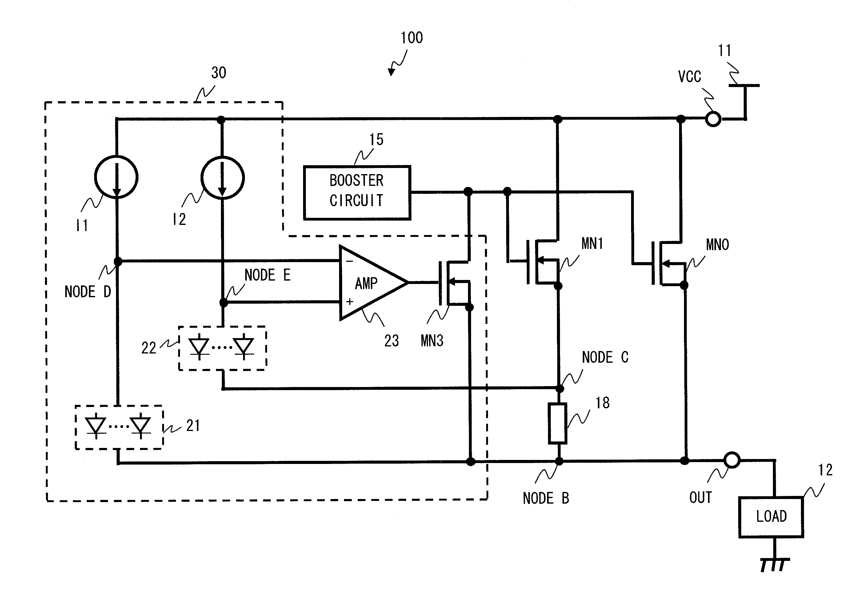
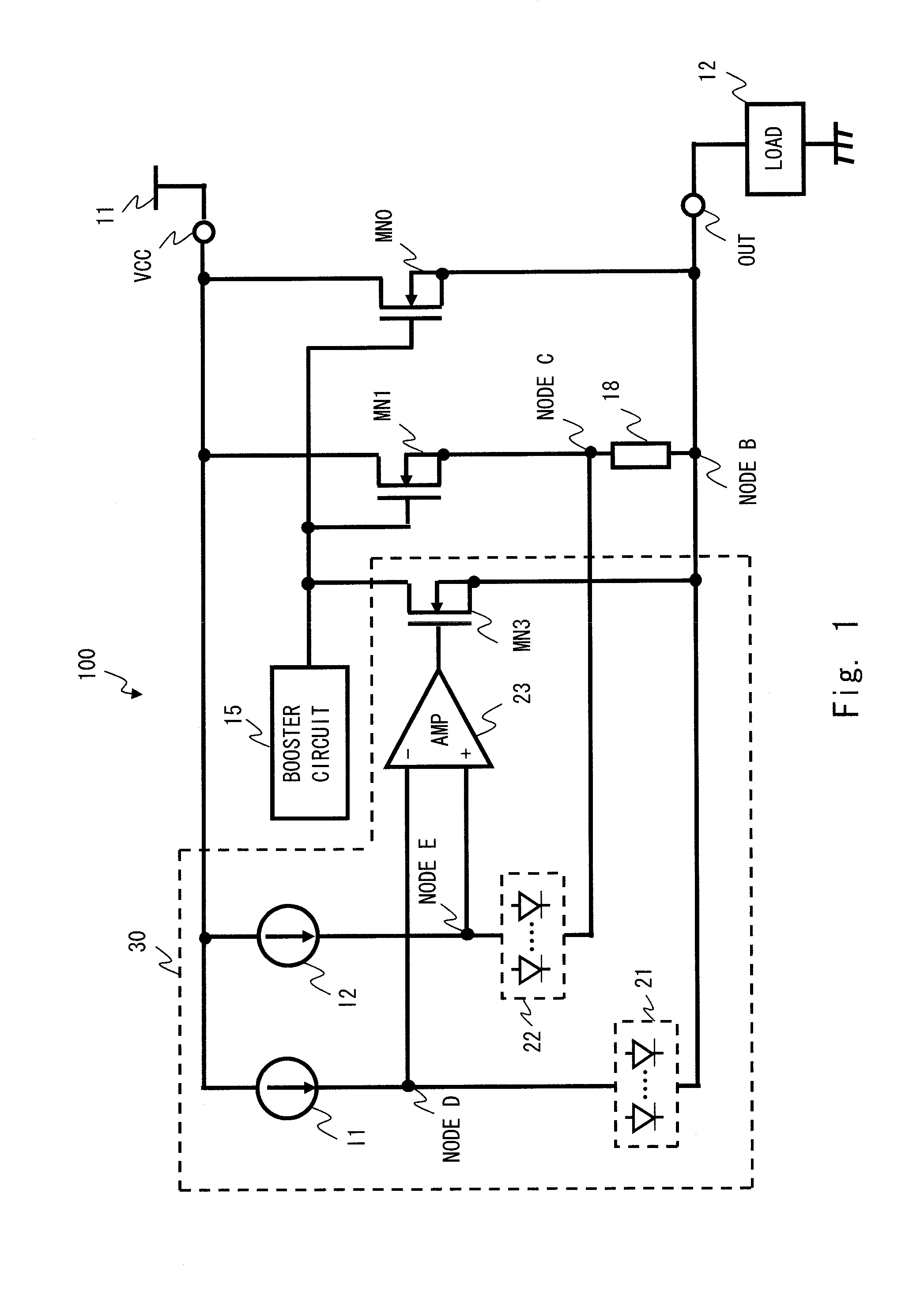
[0035]FIG. 1 shows a current limiting circuit 100 according to an exemplary embodiment of the present invention. The current limiting circuit 100 shown in FIG. 1 includes an output transistor (hereinafter, referred to simply as “transistor”) MN0, a transistor (current sense transistor) MN1, a booster circuit 15, a sense resistor 18, and a determination circuit 30. The first exemplary embodiment exemplifies a case where the transistor MN0 and the transistor MN1 are N-channel MOS transistors.

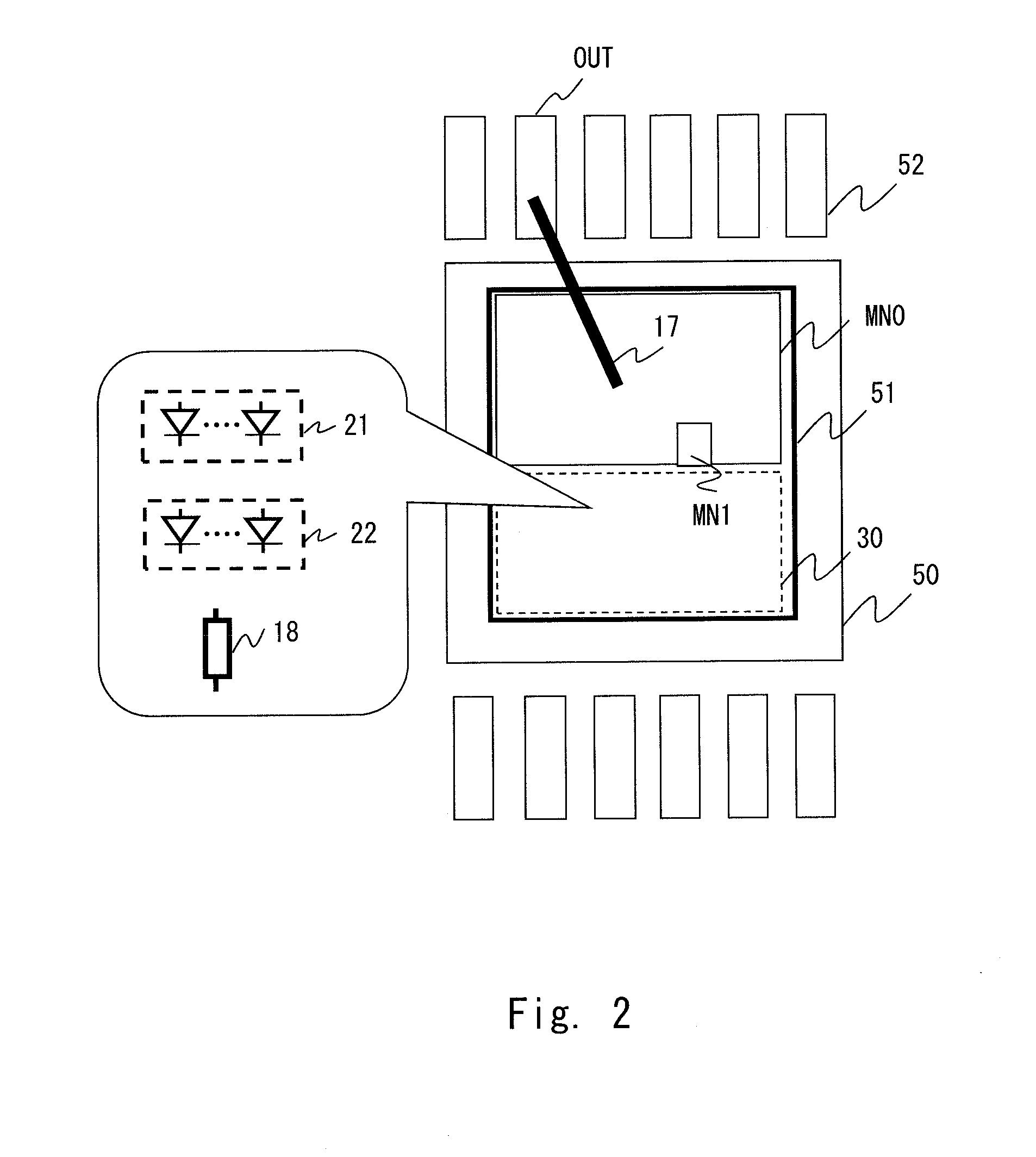
[0036]The sense resistor 18 is formed of a metal having a high heat conductivity. Specifically, the sense resistor 18 is formed of aluminum, copper, or an alloy containing at least one of these elements as a main component.

[0037]First, an exemplary configuration of the circuit shown in FIG. 1 will be described. The transistor MN0 is provided between a high-potential-side power supply terminal VCC and an output terminal OUT. The high-potential-side power supply terminal VCC is supplied with a high-...

second exemplary embodiment

[0059]In the current limiting circuit 100 of the first exemplary embodiment, the diode groups 21 and 22 disposed between the high-potential-side power supply terminal VCC and the output terminal OUT contribute to improvement of the temperature characteristic. However, when the diodes are connected in cascade, it is difficult for the current limiting circuit 100 of the first exemplary embodiment to operate in the state where the voltage level of the high-potential-side power supply 11 is low. In view of this, a current limiting circuit 101 of a second exemplary embodiment of the present invention employs a circuit configuration in which the diode groups 21 and 22 are not used.

[0060]FIG. 4 is a circuit diagram showing the current limiting circuit 101 according to the second exemplary embodiment. The circuit shown in FIG. 4 includes a transistor (first potential difference detecting transistor) MN4, a transistor (second potential difference detecting transistor) MN5, a transistor (firs...


PUM


Abstract

An exemplary aspect of the present invention is a current limiting circuit including: an output transistor that controls a current flowing to a load from a power supply; a current sense transistor through which a current dependent on a current flowing through the output transistor flows; a sense resistor connected in series with the current sense transistor; a potential difference detection unit that detects a potential difference generated between both ends of the sense resistor; a constant current generation unit that supplies a constant current to the potential difference detection unit; and a control unit that controls a conduction state of the output transistor based on a control voltage generated based on the potential difference and the constant current, in which the sense resistor is disposed so as to surround the potential difference detection unit.

Description

INCORPORATION BY REFERENCE[0001]This application is based upon and claims the benefit of priority from Japanese patent application No. 2010-028004, filed on Feb. 10, 2010, the disclosure of which is incorporated herein in its entirety by reference.BACKGROUND[0002]1. Field of the Invention[0003]The present invention relates to a current limiting circuit, and more particularly, to protection against overcurrent in an output transistor.[0004]2. Description of Related Art[0005]A power supply semiconductor is known as a circuit that controls supply of power to a load from a power supply. In the power supply semiconductor, an N-channel MOS transistor is used as an output transistor for a high-side switch, for example.[0006]The power supply semiconductor for use in an LSI (Large Scale Integration) for automotive electrical equipment needs to be protected so as not to be damaged, even if an abnormality such as short-circuiting of a harness to ground occurs.[0007]For example, if the covering...

Claims


Application Information

Patent Timeline
IPC IPC(8): G05F1/10
CPCG05F1/10H03K17/0822H01L2224/48247
Inventor NAKAHARA, AKIHIRO
Owner RENESAS ELECTRONICS CORP
Why Eureka
Eureka Blog
Learn More