
Photodiode, photodiode-equipped display device, and fabrication method therefor

a technology of photodiodes and display devices, applied in non-linear optics, instruments, optics, etc., can solve the problems of variable inability to accurately align resist patterns, and irregular output properties of individual photodiodes, so as to reduce the variations in reduce the effect of channel length shortened, and contribute to the properties of photodiodes

Inactive Publication Date: 2011-08-11
SHARP KK
View PDF5 Cites 2 Cited by
  • Summary
  • Abstract
  • Description
  • Claims
  • Application Information

AI Technical Summary

Benefits of technology

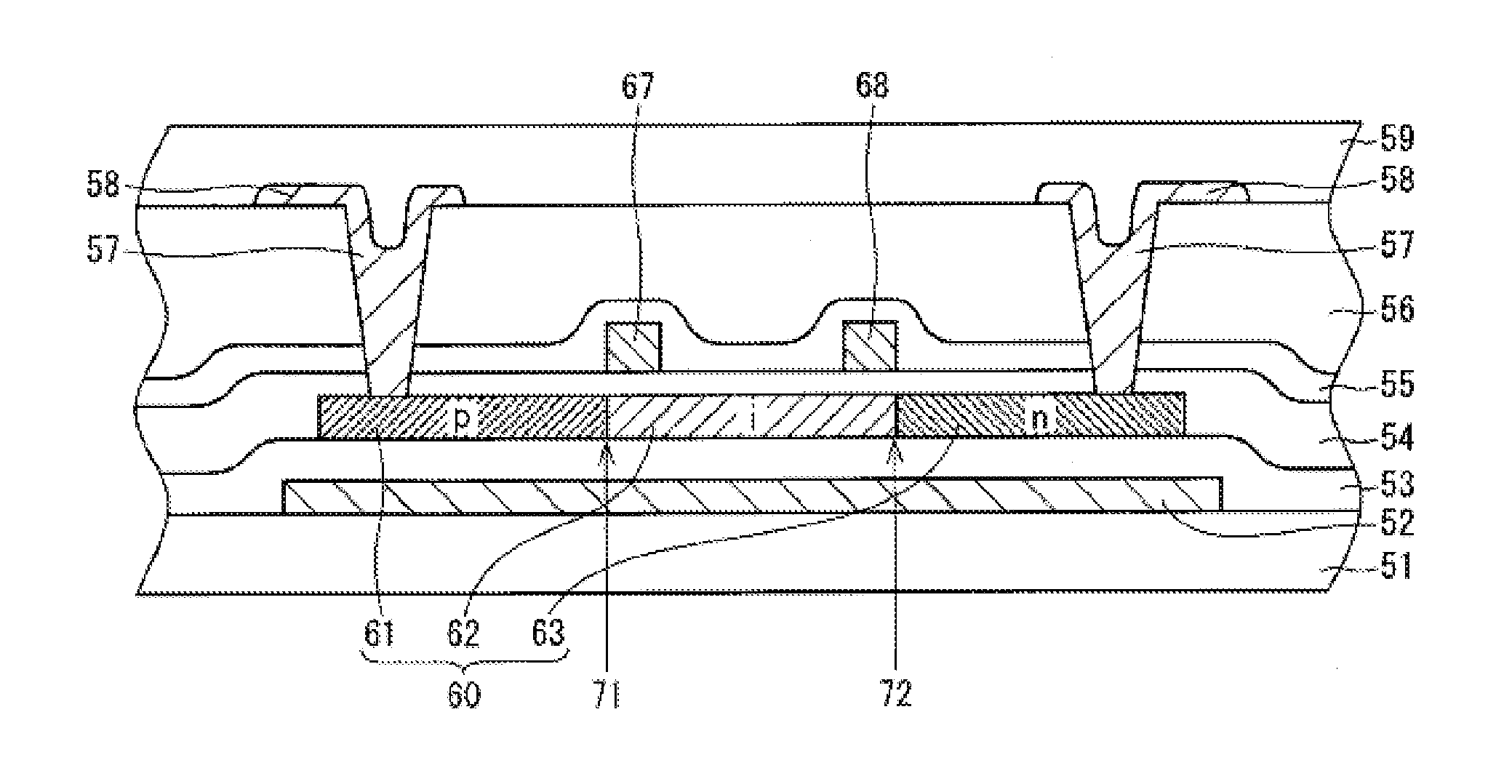
A high precision of channel length of a photodiode can be achieved according to the technology disclosed in FIG. 6 described above. However, in this method, the metal wirings 67 and 68, which were conventionally not formed, are formed over the i-type semiconductor region 62. As a result, the aperture ratio of the display is lowered. Also, when the two smallest diodes formed in accordance with the minimum design rule are compared, with the metal wirings 67 and 68 formed on one of them, the comparison result would indicate that the channel length was shortened by a distance corresponding to the minimum line widths of the metal wirings 67 and 68. This leads to a reduction in the light-receiving area.
Accordingly, there provided is a photodiode that: has a channel width, which contributes to the photodiode properties, as designed; is capable of reducing the variations in the properties of photodiodes in the case that a number of photodiodes are formed; is capable of suppressing the channel length from being shortened; and is capable of minimizing the aperture ratio reduction. Also, a display device equipped with such photodiode, and the fabrication method of the same can be provided.

Problems solved by technology

Irregular channel length causes irregular output properties.
The alignment precision of the resist pattern, however, is not necessarily high, and as a result, the output properties of individual photodiodes are variable.

Method used


Image

  • Photodiode, photodiode-equipped display device, and fabrication method therefor
  • Photodiode, photodiode-equipped display device, and fabrication method therefor
  • Photodiode, photodiode-equipped display device, and fabrication method therefor

Examples


Embodiment Construction

Embodiments of the present invention are described below. The description below includes various limitations preferred for carrying out the present invention. However, the scope of the present invention is not limited to the embodiments and figures below.

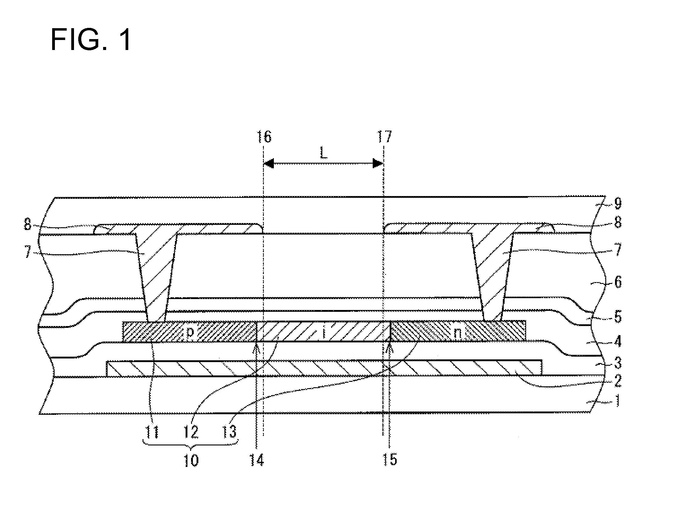
FIG. 1 is a view that shows the structure of a photodiode of the present invention, in which a cross section of the photodiode is illustrated. In FIG. 1, for simpler illustration of the photodiode of the present invention, some dimensions of components are shown enlarged than the actual dimensions, and the size of each component does not reflect the actual size.

In FIG. 1, “1” denotes a substrate made of a material such as glass. This substrate is identical to the substrate on which active elements such as TFTs (not shown) for driving the display device are disposed, and is also called an active matrix substrate. Base coat insulating film 3 is disposed on the substrate 1, and photodiode 10 is disposed on the base coat insulating film...


PUM


Abstract

A photodiode (10) of the present invention has a p-type semiconductor region (11), an i-type semiconductor region (12), and an n-type semiconductor region (13). The channel length “L” of the photodiode (10) is determined by the source wiring films (8) formed by etching. This configuration provides a display device equipped with the plurality of photodiodes (10) having consistent properties.

Description

TECHNICAL FIELDThe present invention relates to a photodiode, a photodiode-equipped display device and a fabrication method for the same. More particularly, the present invention relates to a photodiode preferably used for a liquid crystal display device having a plurality of active elements and driven by the active elements, a display device equipped with the photodiode, a method for fabricating the photodiode, and a method of making a display device equipped with the photodiode.BACKGROUND ARTLiquid crystal display devices are used in a wide variety of equipment. Devices utilizing photodiodes are increasingly diversified, and so is the environment in which the liquid crystal display devices are used. Superior operability under versatile environment as well as energy-saving features are strongly in demand. Liquid crystal display devices themselves offer an increasing range of functions nowadays, expanding their application field.An example of a multi-functional liquid crystal displa...

Claims


Application Information

Patent Timeline
IPC IPC(8): G02F1/13H01L29/04H01L33/08
CPCG02F1/13318G02F2001/13312G02F2201/58Y02E10/50H01L31/022408H01L31/105H01L31/1872H01L27/1446G02F1/13312
Inventor OKAJIMA, NAMIFUJIWARA, MASAHIRO
Owner SHARP KK
Learn More