Semiconductor device and method of producing semiconductor device

a semiconductor device and semiconductor technology, applied in the direction of semiconductor devices, basic electric elements, electrical appliances, etc., can solve the problems of increasing manufacturing costs and difficulty in and achieve the effect of reducing the size of semiconductor devices and the manufacturing cost of semiconductor devices

Inactive Publication Date: 2011-08-25
LAPIS SEMICON CO LTD
View PDF1 Cites 5 Cited by
  • Summary
  • Abstract
  • Description
  • Claims
  • Application Information

AI Technical Summary

Benefits of technology

As described above, in the present invention, it is possible to reduc

Problems solved by technology

As a result, it is necessary to perform the additional step of forming the mask, thereby increasi

Method used


Image

  • Semiconductor device and method of producing semiconductor device
  • Semiconductor device and method of producing semiconductor device
  • Semiconductor device and method of producing semiconductor device

Examples


Embodiment Construction

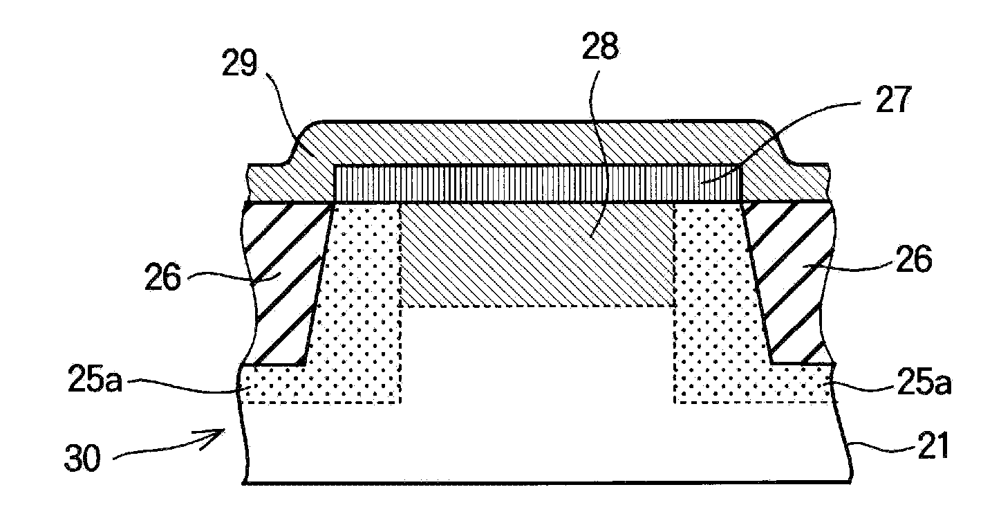
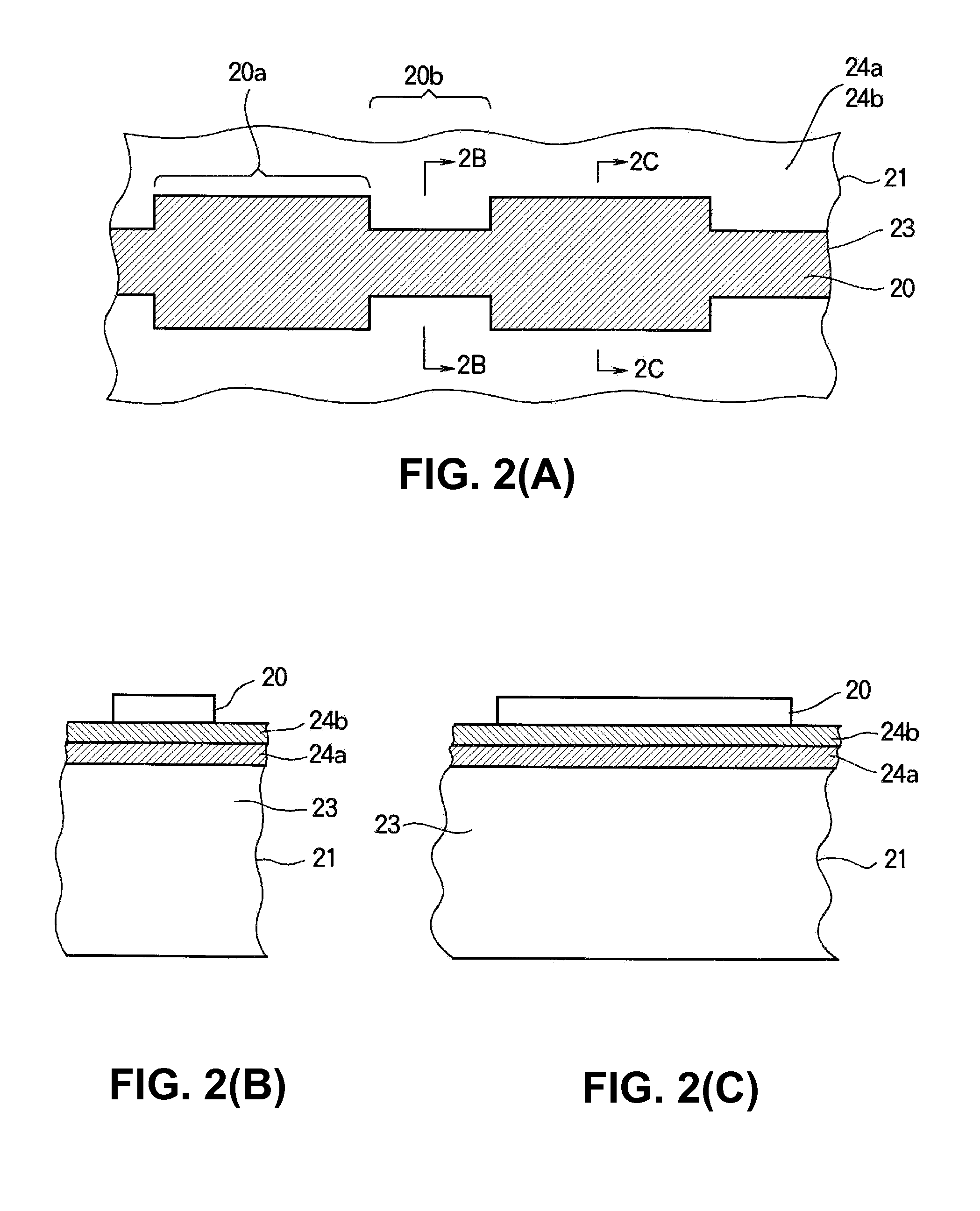
Hereunder, preferred embodiments of the present invention will be explained with reference to the accompanying drawings FIGS. 2(A) to 2(C) to FIGS. 8(A) to 8(C).

FIGS. 2(A) to 2(C) are schematic views No. 1 showing a method of producing a semiconductor device according to an embodiment of the present invention. More specifically, FIG. 2(A) is a schematic plan view thereof, FIG. 2(B) is a schematic sectional view thereof taken along a line 2B-2B in FIG. 2(A), and FIG. 2(C) is a schematic sectional view thereof taken along a line 2C-2C in FIG. 2(A).

In the method of producing the semiconductor device according to an embodiment of the present invention, first, as shown in FIGS. 2(A) to 2(C), a P-type silicon (Si) substrate 21 is prepared as a semiconductor substrate of a first conductive type. In the next step, a silicon oxide film 24a and a silicon nitride film 24b are formed on an entire area of a main surface (an upper surface in FIGS. 2(B) and 2(C)) of the P-type silicon substrate 21...


PUM


Abstract

A method of producing a semiconductor device includes the steps of forming a trench in a semiconductor substrate of a first conductive type so that an active region having a first portion and a second region is formed; implanting a first impurity of the first conductive type at an implantation angle between 30 degrees and 45 degrees relative to a normal line in an implantation direction rotating relative to the normal line so that a first channel diffusion region and a channel stopper region of the first conductive type are formed; filling the trench with an insulation layer; implanting a second impurity of a second conductive type so that a second channel diffusion region of the second conductive type is formed; forming a gate insulation film on the first portion and the second portion; and forming a gate electrode on the gate insulation film.

Description

BACKGROUND OF THE INVENTION AND RELATED ART STATEMENTThe present invention relates to a semiconductor device and a method of producing the semiconductor device. More specifically, the present invention relates to a semiconductor device including a semiconductor integrated circuit, in which a field effect transistor (FET) of an enhancement type and a field effect transistor (FET) of a depletion type are formed, and a method of producing the semiconductor device.A field effect transistor (FET) has been widely used as a transistor of a semiconductor integrated circuit such as a decoder circuit of a semiconductor storage unit such as an ROM (Read Only Memory). Such a semiconductor integrated circuit is mainly configured such that a field effect transistor (FET) of an enhancement type and a field effect transistor (FET) of a depletion type are integrated (refer to Patent Reference).Patent Reference: Japanese Patent Publication No. 11-174405FIGS. 1(A) and 1(B) are schematic plan views sho...

Claims


Application Information

Patent Timeline
IPC IPC(8): H01L21/336
CPCH01L21/26586H01L27/0883H01L21/823493H01L21/823481
Inventor KAMOSHITA, JUNICHI
Owner LAPIS SEMICON CO LTD
Why Eureka
Try Eureka