Method of manufacturing thin-film light-absorbing layer, and method of manufacturing thin-film solar cell using the same
a technology of solar cells and light-absorbing layers, which is applied in the field of manufacturing a thin-film light-absorbing layer and a manufacturing method of a thin-film solar cell using the same, can solve the problems of large-area solar cell production, difficult to make one with a large area, and expensive equipment, and achieves the effect of simple and inexpensive manufacturing
- Summary
- Abstract
- Description
- Claims
- Application Information
AI Technical Summary
Benefits of technology
Problems solved by technology
Method used
Image
Examples
example 1
Formation of CIS-Based Thin-Film Light-Absorbing Layer
[0055]Preparation of Mixture Solution
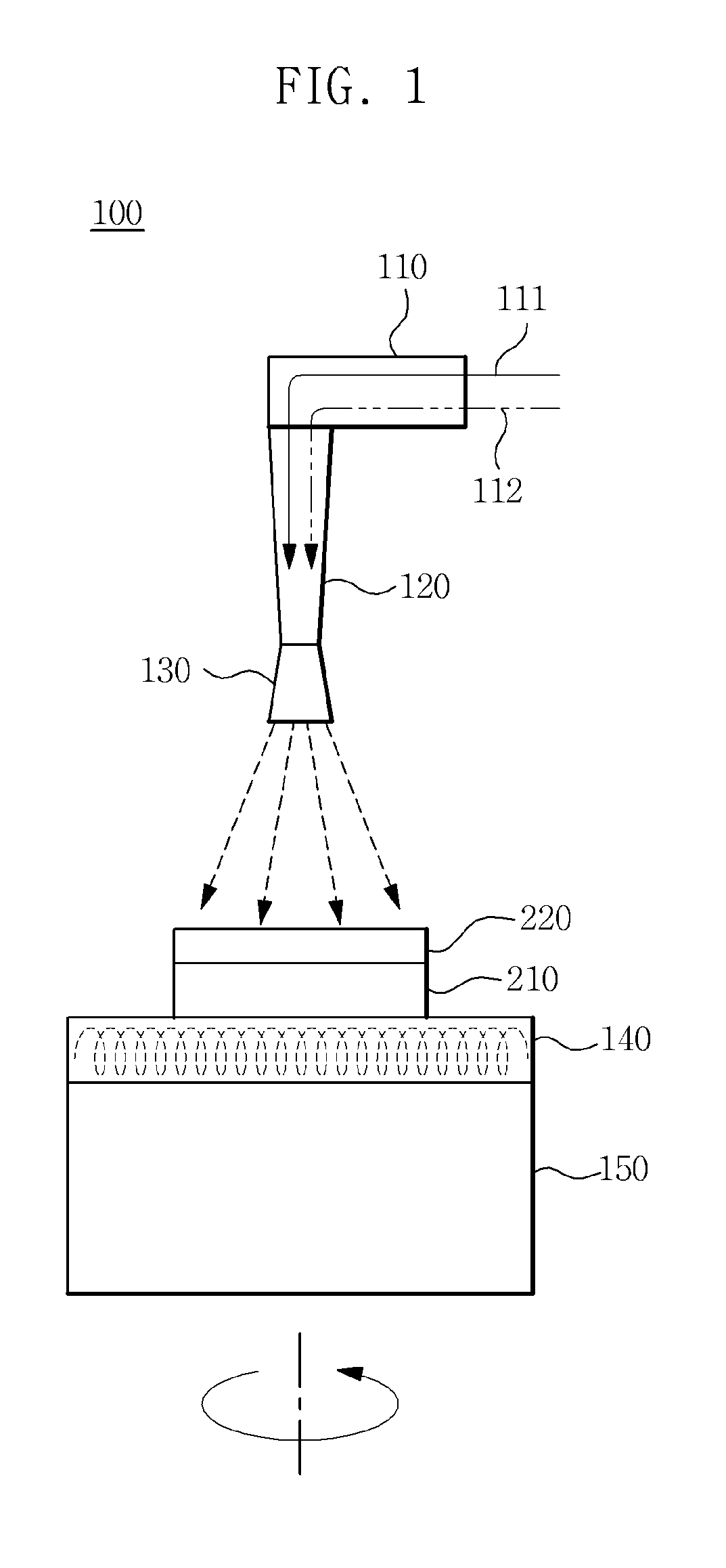
[0056]CuCl2, InCl3 and SeC(NH2)2 precursor solutions were blended in a nitrogen atmosphere so that as little contaminant as possible was added and then mixed at room temperature for about 5 min so that the reaction of respective reactants efficiently occurred, thus preparing a mixture solution represented by CuXInYSeZ (X=0.5˜1.4, Y=0.5˜1.4, Z=1˜6).
[0057]Formation of Thin Film
[0058]Nitrogen gas was controlled so as to be uniformly sprayed at 3˜50 ml / h on a Mo back contact layer heated at 300˜500° C. for 30˜60 min, and the substrate located under the Mo back contact layer was rotated at 10˜50 rpm, whereby the mixture solution was sprayed thereon, and the thin film thus formed was dried by being slowly cooled to room temperature at a rate of 8˜12° C. / min, thus manufacturing a thin film 1 μm thick.
[0059]Selenization
[0060]The thin film was selenized in a Se atmosphere at 450˜610° C. for 30˜120 min,...
example 2
Formation of CIGS-Based Thin-Film Light-Absorbing Layer
[0061]A thin-film light-absorbing layer was manufactured in the same manner as in Example 1, with the exception that GaCl3 was further added to the mixture solution so that the mixture solution contained Ga which replaces some percentage (20%) of In.
example 3
Fabrication of CIS-Based Thin-Film Solar Cell
[0062]Formation of Back Contact Layer
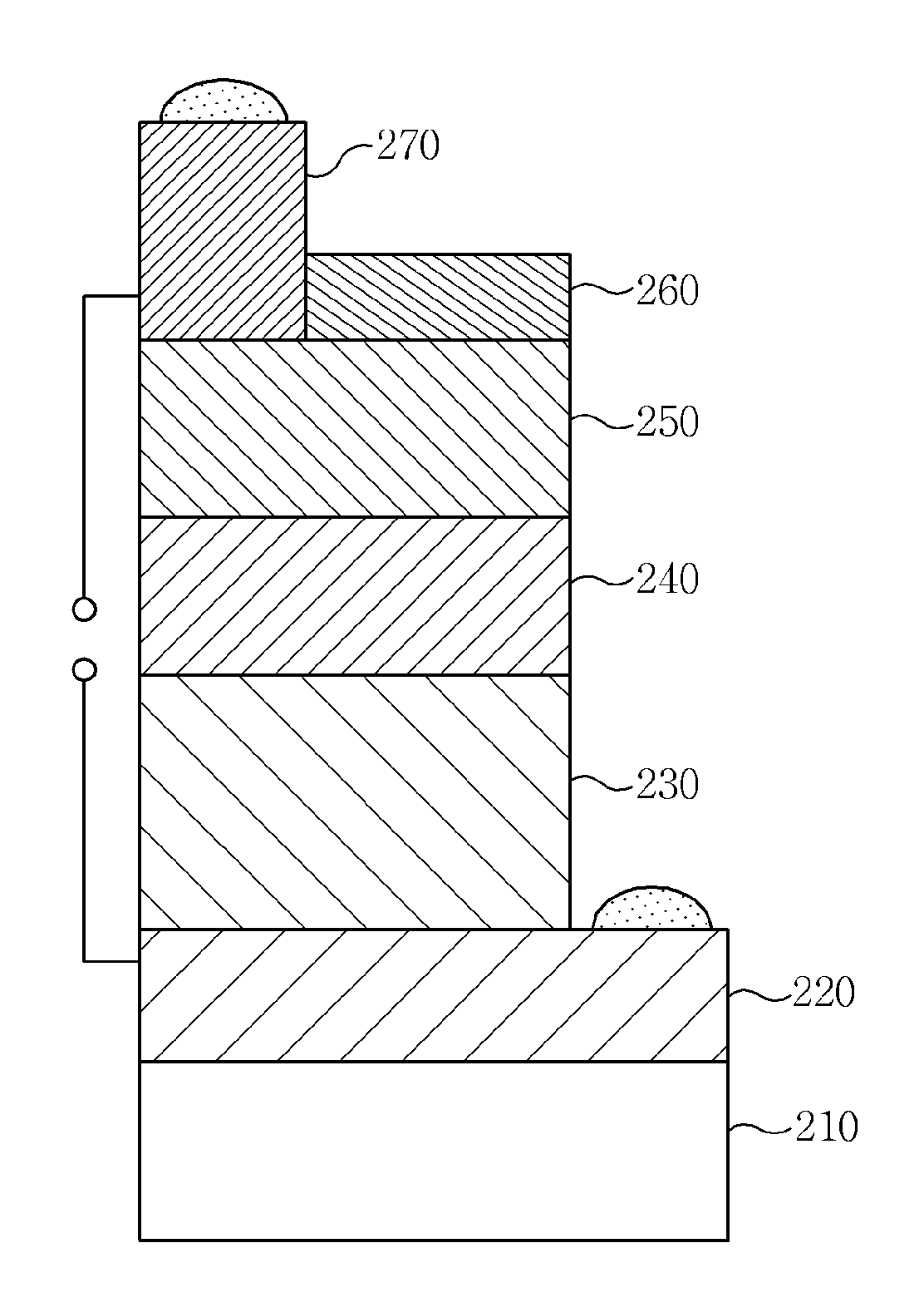
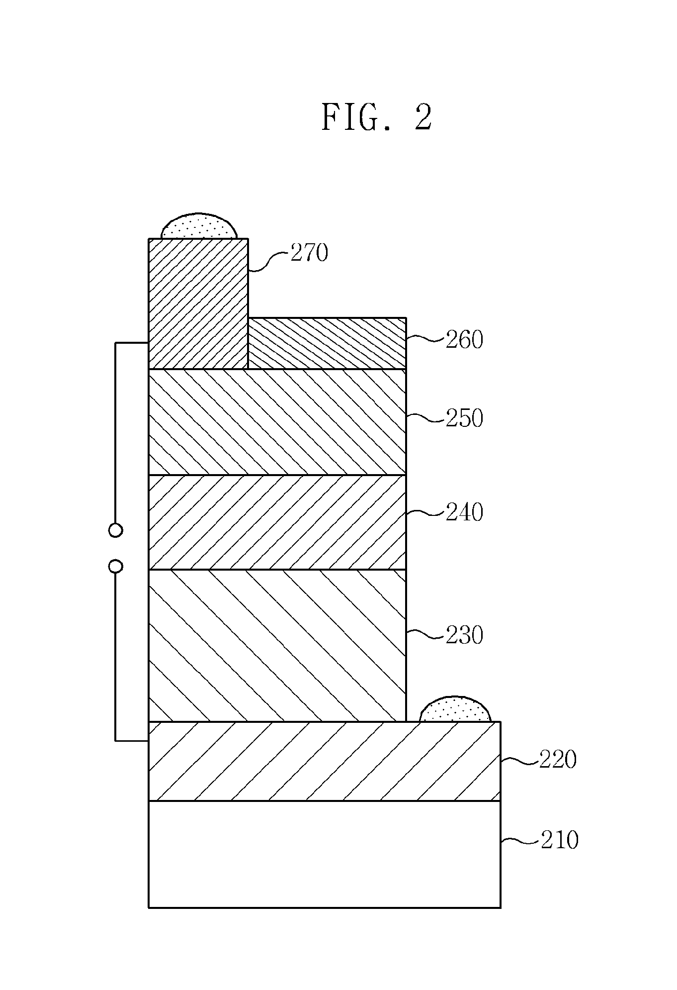
[0063]Mo was deposited to a thickness of 1 μm on a glass substrate or a sodalime glass substrate using sputtering, thus forming a Mo back contact layer.
[0064]Formation of CIS-Based Light-Absorbing Layer
[0065]The CIS-based thin-film light-absorbing layer was formed to a thickness of 1 μm using the procedures of Example 1.
[0066]Formation of Buffer Layer
[0067]A CdS buffer layer was formed on the light-absorbing layer using chemical vapor deposition.
[0068]Formation of Window Layer
[0069]On the buffer layer, i-ZnO and n-ZnO were sequentially deposited using sputtering, thus forming a window layer.
[0070]Formation of Upper Electrode Layer
[0071]An Al upper electrode layer was formed to a thickness of 1 μm on the window layer using sputtering, thereby manufacturing a CIS-based thin-film solar cell.
PUM
| Property | Measurement | Unit |
|---|---|---|
| thickness | aaaaa | aaaaa |
| energy gap | aaaaa | aaaaa |
| temperature | aaaaa | aaaaa |
Abstract
Description
Claims
Application Information
 - R&D
- Intellectual Property
- Life Sciences
- Materials
- Tech Scout
- Unparalleled Data Quality
- Higher Quality Content
- 60% Fewer Hallucinations
Browse by: Latest US Patents, China's latest patents, Technical Efficacy Thesaurus, Application Domain, Technology Topic, Popular Technical Reports.
© 2025 PatSnap. All rights reserved.Legal|Privacy policy|Modern Slavery Act Transparency Statement|Sitemap|About US| Contact US: help@patsnap.com


