Light emitting device

a light-emitting device and light-emitting technology, which is applied in the direction of semiconductor devices, basic electric elements, electrical equipment, etc., can solve the problems of shortening the life of leds, difficult to maintain air tightness, and shrinkage of conductive resins during hardening, and achieve excellent radiation performance and high air tightness

Inactive Publication Date: 2011-09-08
SEIKO INSTR INC
View PDF6 Cites 19 Cited by
  • Summary
  • Abstract
  • Description
  • Claims
  • Application Information

AI Technical Summary

Benefits of technology

[0011]It is an object of the present invention to provide a light emitting device which has h

Problems solved by technology

However, as in reference application 1, when the conductive resin is filled into the through holes and hardened to form the through-electrodes, shrinkage of the conductive resin occurs during hardening.
Therefore, it has been difficult to maintain airtightness.
Further, the LED generates heat during light emission.
As a result

Method used


Image

  • Light emitting device
  • Light emitting device
  • Light emitting device

Examples


first example

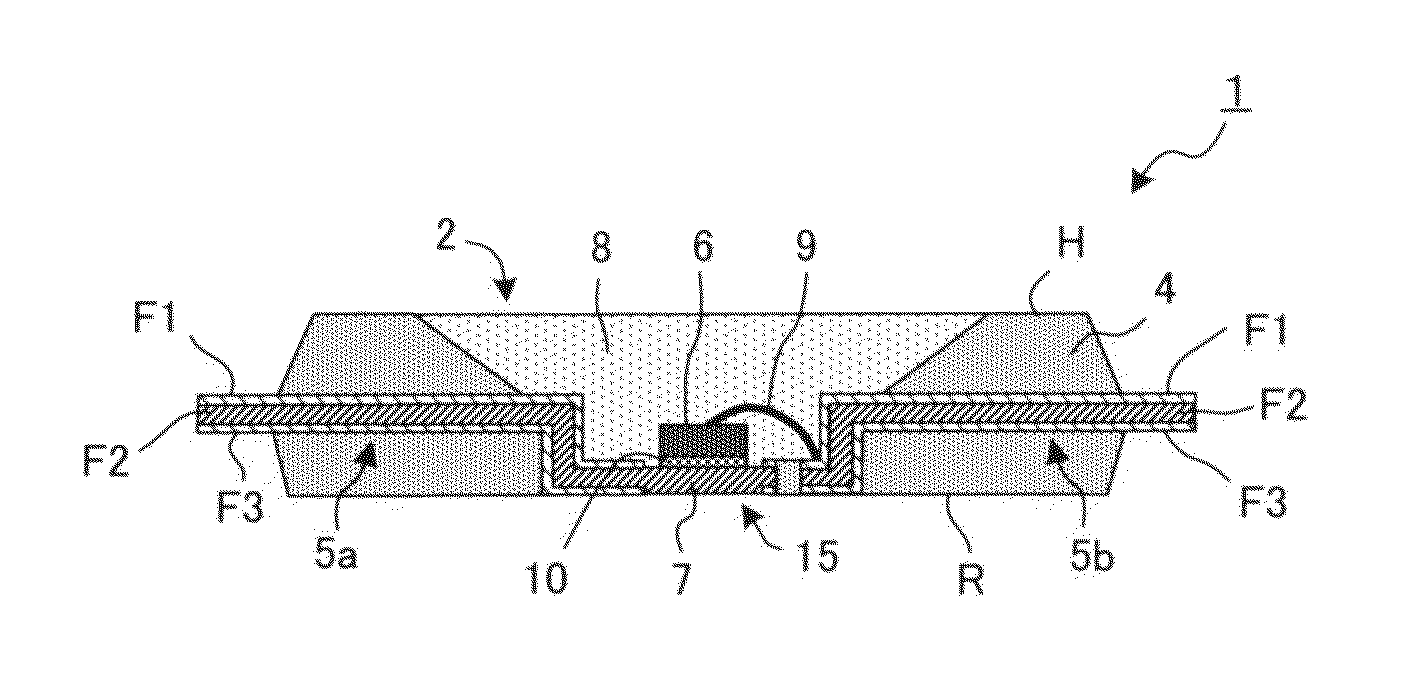
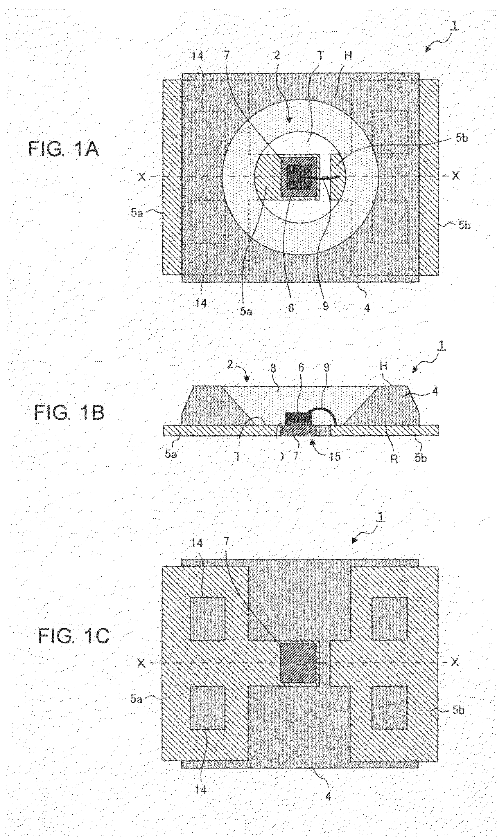
[0030]A light emitting device 1 according to a first example is described with reference to FIGS. 1A to 1C. FIG. 1A is a schematic top view of the light emitting device 1, FIG. 1B is a schematic view of a cross section taken along the line XX of FIG. 1A or FIG. 1C, and FIG. 1C is a schematic view seen from the rear side of the light emitting device 1. As is apparent from FIGS. 1A to 1C, a light emitting element 6 is mounted on a copper material 7 which is embedded in a lead frame 5a so as to pass through the lead frame 5a. A glass substrate 4 and the lead frame 5a are bonded to each other so that the light emitting element 6 is exposed from a recess (opening) 2 of the glass substrate 4.

[0031]As illustrated in FIGS. 1A to 1C, in the light emitting device 1, the lead frame 5a and a lead frame 5b are bonded to a rear surface R of the glass substrate 4. The recess 2 is formed in a front surface H of the glass substrate 4. The light emitting element 6 is mounted on a part of the lead fra...

second example

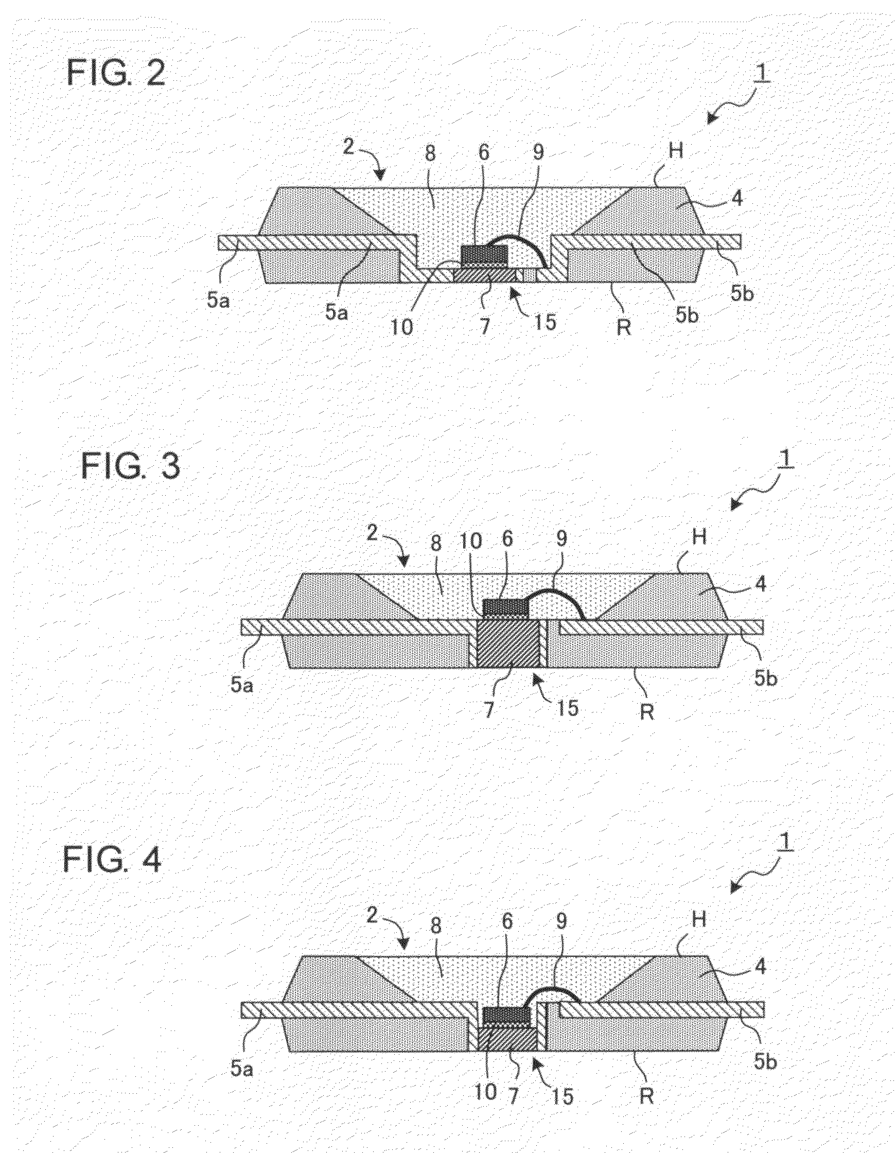
[0038]FIG. 2 is a schematic vertical cross-sectional view of a light emitting device 1 according to a second example. The second example differs from the first example in the shape of the lead frames 5a and 5b. Other structures are the same as those in the first example, and hence overlapping description is omitted. In this example, the lead frames 5a and 5b are embedded in the glass substrate 4. As illustrated in FIG. 2, one end of each of the lead frames 5a and 5b is exposed from the bottom surface of the recess 2 and from the rear surface R of the glass substrate 4, and another end thereof is protruded from the side surface of the glass substrate 4 (at a middle portion in height between the front surface H and the rear surface R). The one end of each of the lead frames 5a and 5b is bent toward the rear surface R side of the glass substrate 4 at a bottom portion of the recess 2. The upper surfaces of the lead frames are formed to be flush with the bottom surface of the recess 2, a...

third example

[0040]FIG. 3 is a schematic vertical cross-sectional view of a light emitting device 1 according to a third specific example. The third example differs from the second example in that the mounting portion 15 of the lead frame 5a, on which the light emitting element 6 is mounted, is formed to be thicker than other portions. Other structures are the same as those in the second example, and hence overlapping description is omitted as appropriate. By forming the mounting portion 15 of the lead frame 5a thicker than the other portions, the length of the bonding surface with the copper material embedded in the lead frame or the length of the bonding surface between the lead frame and the glass substrate is increased, and hence airtightness is improved.

[0041]As illustrated in FIG. 3, the lead frame 5a has one end including the mounting portion 15 which is exposed on the bottom surface side of the recess 2 and the rear surface R side of the glass substrate 4, and another end protruded from ...


PUM


Abstract

A light emitting device (1) includes a glass substrate (4) having a recess (2) in a front surface, and a lead frame (5a). A copper material (7) is embedded so that the copper material (7) passes through the lead frame (5a). A light emitting element (6) is mounted on the copper material (7). The glass substrate (4) and the lead frame (5a) are bonded to each other so that the light emitting element (6) is exposed from the recess of the glass substrate (4). Thus, the copper material is embedded in a pass-through manner directly under a region of the lead frame where the light emitting element is disposed. Therefore, adhesion between the glass substrate and the lead frame is ensured, and heat generated by the light emitting element may be efficiently radiated from the rear surface of the glass substrate.

Description

BACKGROUND OF THE INVENTION[0001]1. Field of the Invention[0002]The present invention relates to a light emitting device in which a light emitting element is mounted on a package using a glass material.[0003]2. Description of the Related Art[0004]In recent years, an electronic component using a glass package has been put to practical use. A glass material has high airtightness, and hence it is possible to prevent moisture or contaminants from entering from the outside. Further, the glass material has a thermal expansion coefficient which is close to that of a silicon substrate of a semiconductor element. Therefore, high reliability is ensured at a mounting surface or at a bonding surface when the semiconductor element is mounted on the glass material. Still further, the glass material is low in cost, and hence an increase in product cost may be suppressed.[0005]FIG. 6 schematically illustrates a cross-sectional structure of a conventional LED light emitting device 100. A plurality o...

Claims


Application Information

Patent Timeline
IPC IPC(8): H01L33/62
CPCH01L33/62H01L2224/48091H01L2224/48247H01L2224/73265H01L2924/00014H01L2924/181H01L33/486H01L2924/00H01L2924/12041H01L2924/00012H01L33/647
Inventor TSUKAGOSHI, KOJIKAMAMORI, HITOSHIOKU, SADAOFUJITA, HIROYUKIHAYASHI, KEIICHIRO
Owner SEIKO INSTR INC
Why Eureka
Try Eureka