Display panel and method of manufacturing the same

Inactive Publication Date: 2011-09-08
SAMSUNG DISPLAY CO LTD
View PDF24 Cites 3 Cited by
  • Summary
  • Abstract
  • Description
  • Claims
  • Application Information

AI Technical Summary

Benefits of technology

[0013]When the droplet is sprayed to a desired position by using an inkjet process and the solvent in the droplet is vaporized, the bead spacer may be easily gathered on the area where the droplet is sprayed. Accordingly, the cell gap between the first and second substrates may maintain a uniform distance, thereby improving display properties of the display panel.

Problems solved by technology

However, a nonuniform cell gap between the first and second substrates causes variations in thickness of the liquid crystal layer, thereby distorting the image.
When the bead spacer is applied to the liquid crystal display, there are situations where the uniform cell gap is not maintained because the bead spacer is difficult to form at a desired position.

Method used


Image

  • Display panel and method of manufacturing the same
  • Display panel and method of manufacturing the same
  • Display panel and method of manufacturing the same

Examples


Embodiment Construction

[0028]It will be understood that when an element or layer is referred to as being “on”, “connected to” or “coupled to” another element or layer, it can be directly on, connected or coupled to the other element or layer or intervening elements or layers may be present. Like numbers may refer to like elements throughout the drawings and the specification.

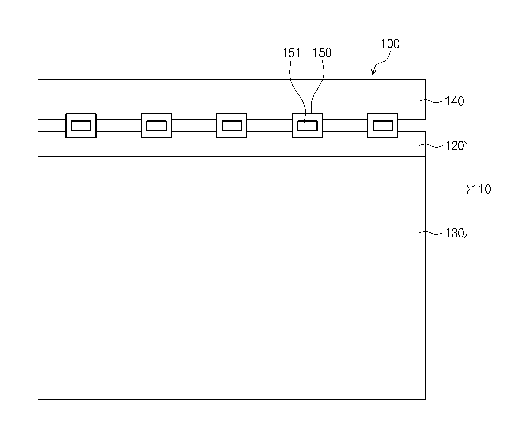
[0029]FIG. 1 is a plan view showing a display unit according to an exemplary embodiment of the present invention.

[0030]Referring to FIG. 1, a display unit 100 includes a display panel 110 displaying an image and a printed circuit board 140 providing the display panel 110 with a driving signal. The printed circuit board 140 is disposed adjacent to a side of the display panel 110.

[0031]The display panel 110 includes a first substrate 120, a second substrate 130 facing the first substrate 120, and a liquid crystal layer (not shown) disposed between the first and second substrates 120 and 130.

[0032]The printed circuit board 140 is connect...


PUM


Abstract

A display panel includes a first substrate, a second substrate facing the first substrate, and a pixel disposed on either the first substrate or the second substrate. When an electrode is formed, a portion of the electrode is removed to form a spacer area and a droplet including a bead spacer mixed with a solvent is provided in the spacer area. Then, the solvent is vaporized to move the bead spacer to a center of the spacer area. The second substrate is provided to face the first substrate while interposing the bead spacer therebetween. The spacer area has a dimension equal to or greater than a diameter of the droplet.

Description

CROSS-REFERENCE TO RELATED APPLICATION[0001]This application claims priority to Korean Patent Application No. 2010-19732 filed on Mar. 5, 2010, the contents of which are herein incorporated by reference in its entirety.BACKGROUND[0002]1. Technical Field[0003]Embodiments of the present invention relate to a display panel including a bead spacer and a method of manufacturing the display panel.[0004]2. Discussion of the Related Art[0005]In general, a liquid crystal display includes a liquid crystal display panel including a first substrate, a second substrate, and a liquid crystal layer interposed between the first and second substrates.[0006]The liquid crystal display displays an image using the liquid crystal layer in which liquid crystal molecules are arranged in response to voltages applied to the first and second substrates. However, a nonuniform cell gap between the first and second substrates causes variations in thickness of the liquid crystal layer, thereby distorting the imag...

Claims


Application Information

Patent Timeline
IPC IPC(8): G02F1/1339G02F1/13
CPCG02F1/1339G02F1/13G02F1/13394G02F1/133512G02F1/13392G02B26/005G02F1/13396
Inventor LEE, JEONGHOSUNG, WOO YONGCHA, TAEWOONKIM, TAEGYUNCHOI, SANGGUNBAE, JIHYUNLEE, HYOUNG WOOK
Owner SAMSUNG DISPLAY CO LTD
Why Eureka
Try Eureka