Multi-Layer LED Array Engine

a technology of led arrays and array engines, which is applied in the direction of semiconductor devices for light sources, semiconductor/solid-state device details, lighting and heating apparatus, etc., can solve the problems of inflexible application of pcb as the substrate for multi-layer led arrays, the size of led products is restricted by the packaged led units, and the inability to dissipate heat generated, etc., to achieve the effect of saving production cost and time and simplifying the operation process

Inactive Publication Date: 2011-09-22
GEM WELTRONICS TWN CORP
View PDF5 Cites 26 Cited by
  • Summary
  • Abstract
  • Description
  • Claims
  • Application Information

AI Technical Summary

Benefits of technology

[0009]Accordingly, a primary objective of the present invention is to provide a multi-layer LED array engine having a multi-layer architecture. The multi-layer architecture of the LED array is simple and adapted for simplifying the operation process and saving production cost and time thereof.
[0015]In some certain circumstances, very high power LED application may be desired, and correspondingly according to an aspect of the present invention, the phosphorous wall and the optical reflectivity surface are sputtered with a nickel or chromium coating. Or alternatively, a metal reflector cap plated with a nickel or chromium coating is provided on the phosphorous wall and the optical reflectivity surface for improving the light reflectivity of the multi-layer LED array engine. Each lead frame includes an inner end, a center part, and an outer end. The center part of each lead frame for wire bonding is sealed inside the protruded plate. The inner end of the lead frame at the lighting area is adapted for internal electrical connection and the outer end of the lead frame is adapted for external electrical connection. Each lead frame 5 is further configured with at least one second locking hole and at least one second locking-in groove between the inner end and the outer end. The second locking-in groove and the second locking hole are buried and sealed inside the molded platform. However, the inner end of the lead frame and the outer end of the lead frame are reserved unsealed by the molded platform for wire bonding and electrical connection. A plurality of holes are configured at the outer end of the lead frame for electrical connection with external components. The outer end of the lead frame is configured extending out beyond the peripheral edge of the base plate frame for external electrical connection.

Problems solved by technology

However, according to the secondary level assembly architecture, the size of the LED products is restricted by the packaged LED unit, since the size of the packaged LED unit is much larger than the size of the die.
However, the leads are usually too thin to be good enough for dissipating the heat generated thereby.
However, a PCB is usually fabricated by many complicated processes including lithographing, stamping, drilling, and plating copper in through holes.
Therefore, the application of PCB as the substrate for the multi-layer LED array is not flexible, since once the PCB is prepared, it cannot be conveniently modified.

Method used


Image

  • Multi-Layer LED Array Engine
  • Multi-Layer LED Array Engine
  • Multi-Layer LED Array Engine

Examples


Embodiment Construction

[0026]The accompanying drawings are included to provide a further understanding of the invention, and are incorporated in and constitute a part of this specification. The drawing illustrates embodiments of the invention and, together with the description, serves to explain the principles of the invention.

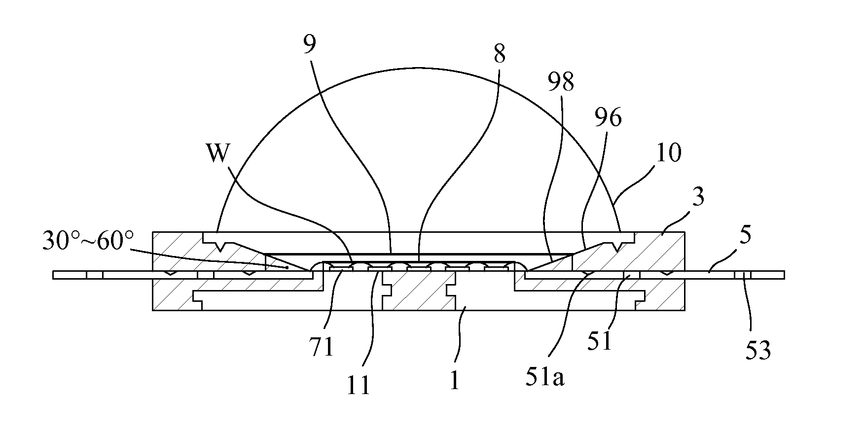
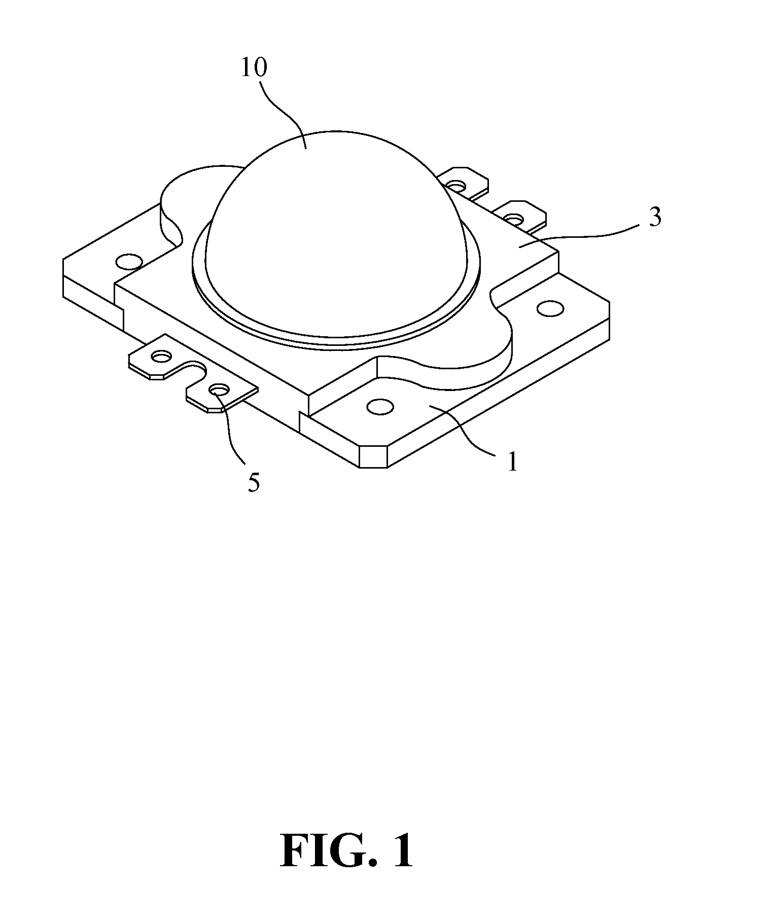
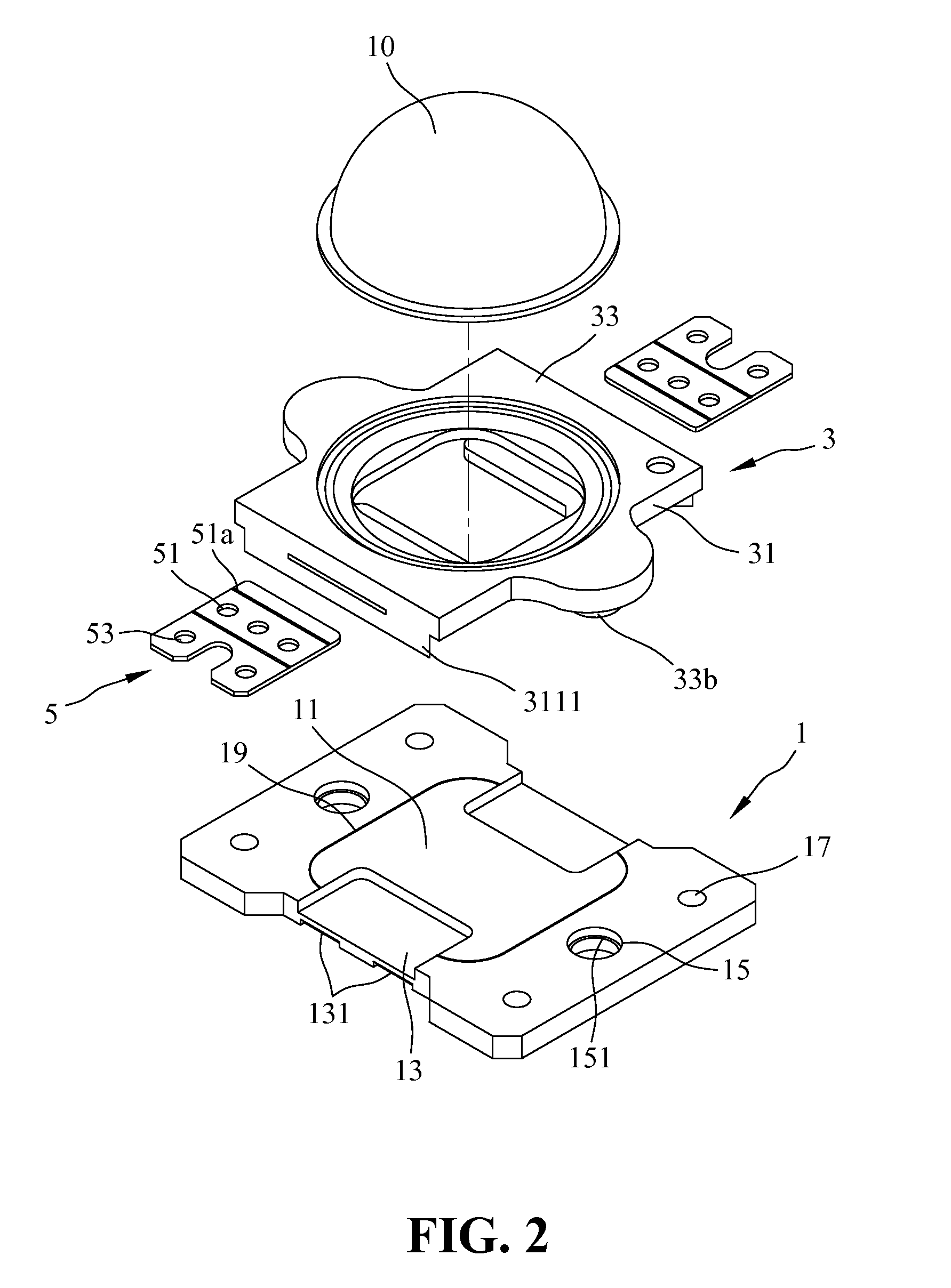
[0027]FIG. 1 is a perspective view of a multi-layer LED array engine according to an embodiment of the present invention. FIG. 2 is an exploded view of the multi-layer LED array engine according to an embodiment of the present invention. FIG. 3 is an exploded cross-sectional view of the multi-layer LED array engine according to an embodiment of the present invention.

[0028]Referring to FIGS. 1 through 3, there is shown a multi-layer LED array engine. The multi-layer LED array engine includes a base plate frame 1, a molded platform 3, at least one lead frame 5, and a dome 10.

[0029]The base plate frame 1 includes at least one lighting area 11 and two lead frame grooves 13. As shown in ...


PUM


Abstract

A multi-layer LED array engine is provided. The multi-layer LED array engine includes a base plate frame, a molded platform, two lead frames, a lighting element, a dome, a protection layer, and a phosphorous layer. The molded platform is disposed on and secured to the base plate frame. The two lead frames are combined with two lead frame grooves of the base plate frame. The lighting element is disposed on a lighting area of the base plate frame. The protection layer is provided on the lighting element, and the phosphorous layer is provided on the protection layer. The dome is secured to the molded platform for covering the molded platform and the lighting element.

Description

BACKGROUND OF THE INVENTION[0001]1. Field of the Invention[0002]The present invention relates generally to a multi-layer light emitting diode (LED) array engine. The multi-layer LED array engine can be fabricated by a very simple manufacturing process with a low manufacturing cost and a short manufacturing cycle time.[0003]2. The Related Arts[0004]Generally, an LED emits light in accordance with the intrinsic characteristic of the solid state semiconductor of the LED. Differing from the light emitting principle of the filament light bulb, an LED emits light when a current flows to the semiconductor PN junction, and does not need to be heated to a high temperature. As such, LEDs are also known as cold light sources. LEDs typically have the advantages including better durability, longer lifespan, lower weight, and lower power consumption. Particularly and more importantly, LEDs do not contain poisonous materials, e.g., mercury or poisonous gases. Therefore, LEDs are often used in form...

Claims


Application Information

Patent Timeline
Patent Type & Authority Applications(United States)
IPC IPC(8): H01L33/00
CPCF21K9/00H01L25/0753H01L2224/48137H01L33/58H01L33/507
Inventor HWU, JON-FWUWU, YUNG-FU
Owner GEM WELTRONICS TWN CORP
Why Eureka
Try Eureka