Internal-clock adjusting circuit

a technology of internal clock and adjusting circuit, which is applied in the direction of generating/distributing signals, single output arrangements, pulse techniques, etc., can solve the problems of long time to reach the locked state, the timing of the edge tends to deviate from the target timing in the locked state, and the phase of the output data slightly lags behind that of the external clock signal. achieve the effect of ensuring both precision and high-speed performan

Inactive Publication Date: 2011-09-22
LONGITUDE SEMICON S A R L
View PDF5 Cites 21 Cited by
  • Summary
  • Abstract
  • Description
  • Claims
  • Application Information

AI Technical Summary

Benefits of technology

[0008]According to the present invention, it makes easier to ensure both precision and high-speed performance in the timing adjustment of the internal clock signal.

Problems solved by technology

However, when the semiconductor device outputs data while using the external clock signal as a timing signal, a phase of the output data slightly lags behind that of the external clock signal because of an operating delay in an output buffer circuit.
However, when a timing of an edge largely deviates from a target timing in an unlocked state, it takes long time to reach the locked state.
However, because of coarse adjustment, the timing of the edge tends to deviate from the target timing in the locked state.

Method used


Image

  • Internal-clock adjusting circuit
  • Internal-clock adjusting circuit
  • Internal-clock adjusting circuit

Examples


Embodiment Construction

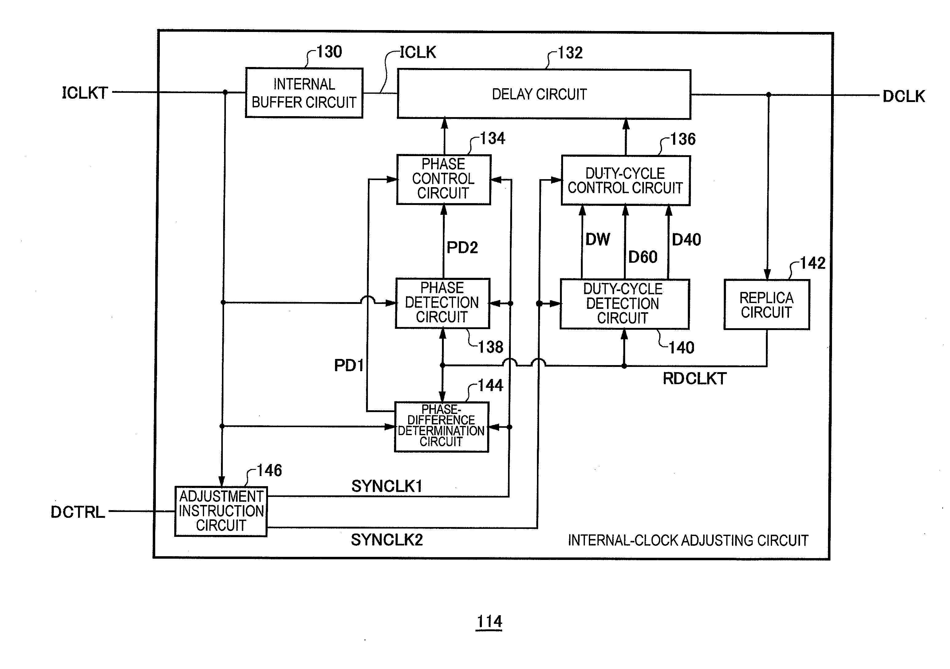
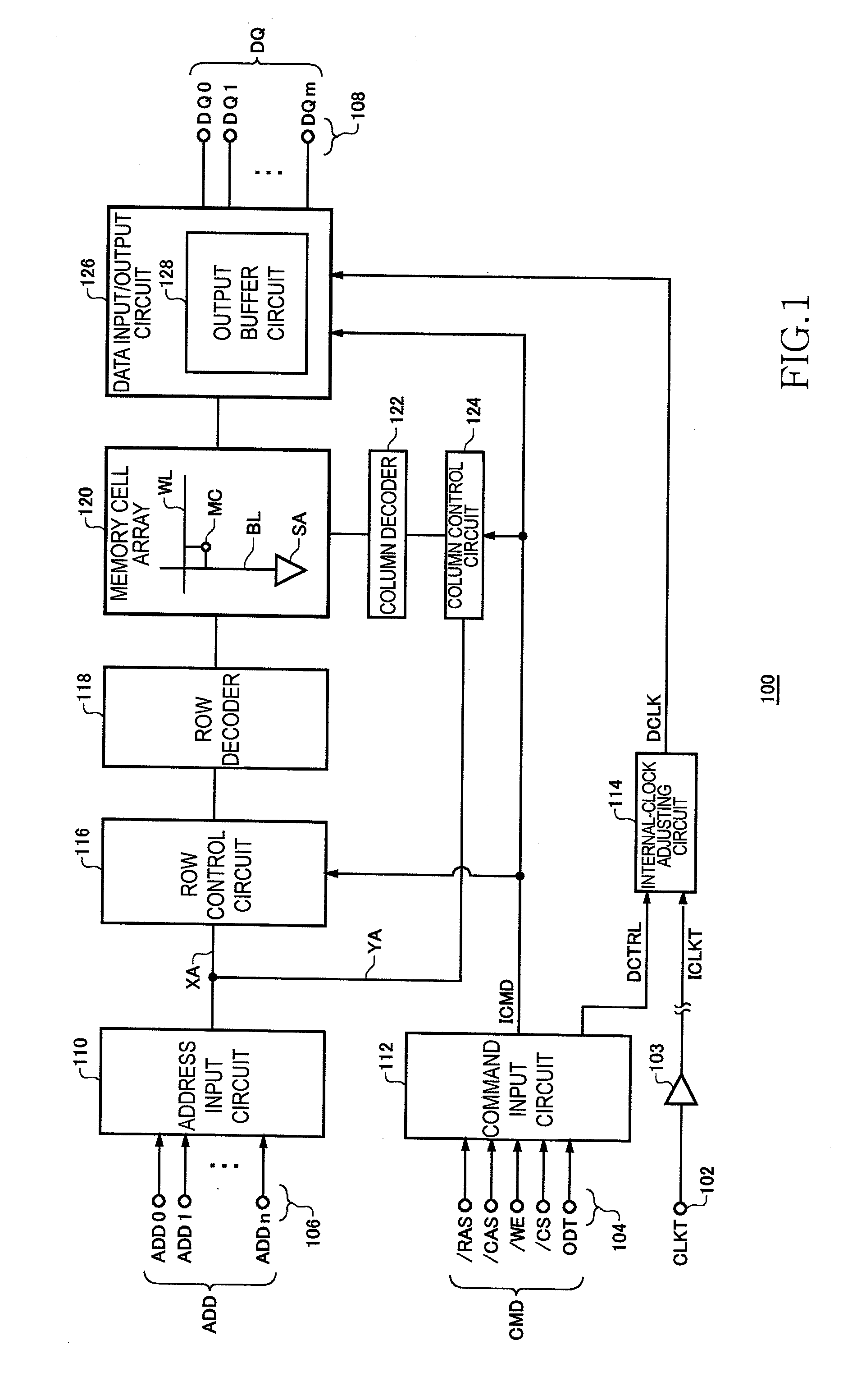
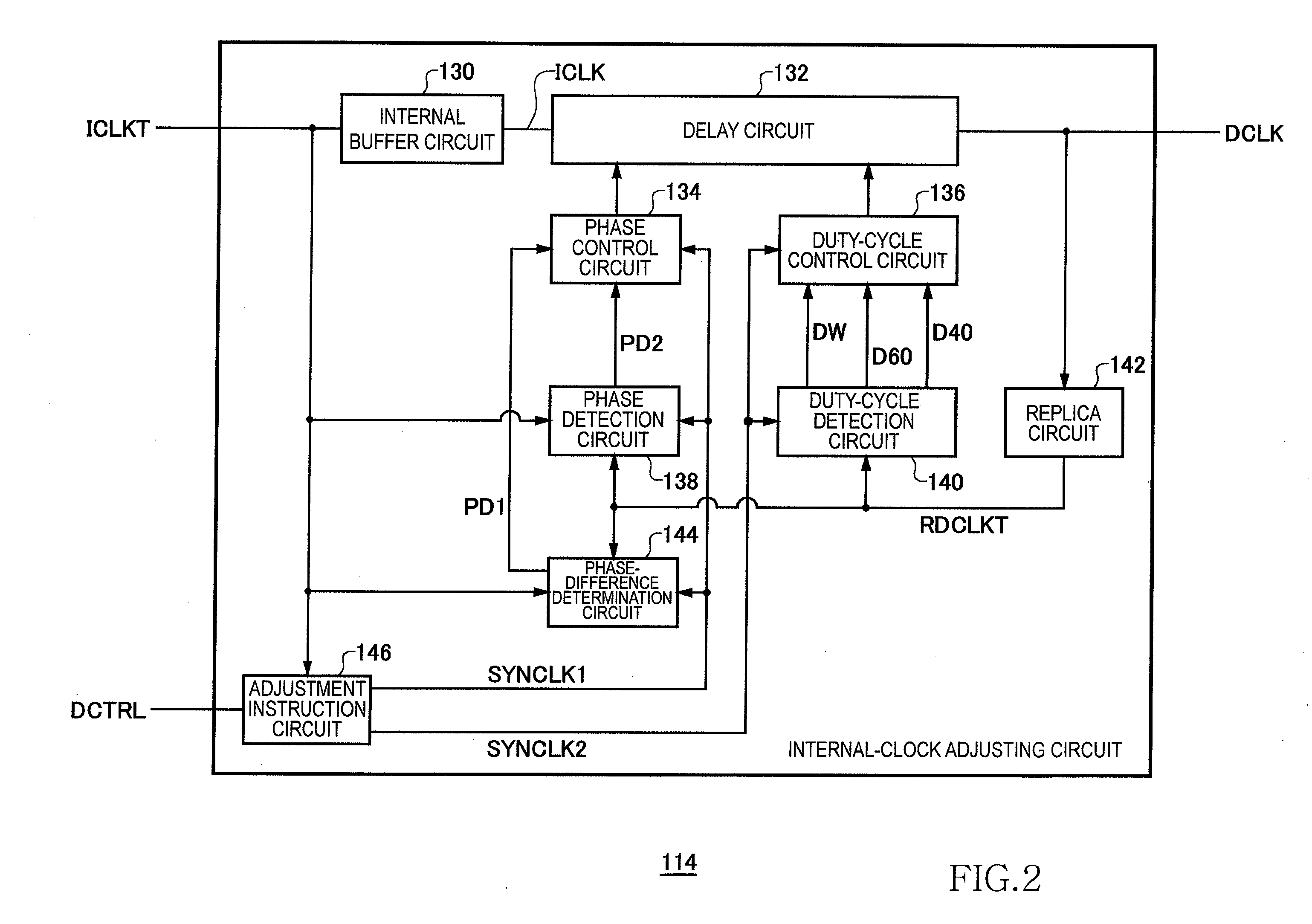
[0019]An internal-clock adjusting circuit generates an internal clock signal so that a phase of an output data matches to that of an external clock signal. The internal-clock adjusting circuit sets an adjustment pitch of a phase adjustment of the internal clock signal to be relatively high when a phase difference between the both clock signals is large, and low when the phase difference is small. Strictly speaking, the external clock signal is a kind of an internal clock signal since the external clock signal is supplied to the internal-clock adjusting circuit via an input receiver within a semiconductor device.

[0020]The internal-clock adjusting circuit controls a duty cycle of the internal clock signal to be closer to 50%. The internal-clock adjusting circuit sets a duty cycle pitch of the internal clock signal to be relatively high when the duty cycle of the internal clock signal largely deviates from 50%, and relatively low when the duty cycle is close to 50%.

[0021]Preferred embo...


PUM


Abstract

A delay circuit generates an internal clock signal or a second clock signal by delaying an external clock signal. A detection-potential generation circuit included in a phase-difference determination circuit generates a detection potential corresponding to a difference between a timing of an active edge of an internal clock signal or a third clock signal and a timing of the target external clock signal in a first node. A reference-potential generation circuit included in the phase-difference determination circuit generates a reference potential in a second node. A phase control circuit delays the second clock signal according to the detection potential. At this time, when the detection potential is higher than the reference potential, an adjustment amount of the second clock signal per adjustment changes.

Description

BACKGROUND OF THE INVENTION[0001]1. Field of the Invention The present invention relates to an internal-clock adjusting circuit to adjust a timing of an internal clock signal.[0002]2. Description of Related Art[0003]Data is input to or output from a semiconductor device such as an SDRAM (Synchronous Dynamic Random Access Memory) synchronously with a clock signal supplied from outside (hereinafter, “external clock signal”). However, when the semiconductor device outputs data while using the external clock signal as a timing signal, a phase of the output data slightly lags behind that of the external clock signal because of an operating delay in an output buffer circuit. To avoid this delay, the semiconductor device often generates an internal clock signal having a phase advanced by an internal-clock adjusting circuit such as a DLL (Delay Locked Loop) circuit by as much as the operating delay, and outputs data while using the internal clock signal as a timing signal.[0004]The internal...

Claims


Application Information

Patent Timeline
Patent Type & Authority Applications(United States)
IPC IPC(8): H03L7/06G06F1/04H03K5/00H03K5/13
CPCG06F1/04
Inventor MIYANO, KAZUTAKA
Owner LONGITUDE SEMICON S A R L
Why Eureka
Try Eureka