Single-electron detection method and apparatus for solid-state intensity image sensors

a single-electron detection and intensity image technology, applied in the field of single-electron detection methods and apparatuses for solid-state intensity image sensors, can solve problems such as limited dynamic range, and achieve the effects of high dynamic range and sensitivity, extended dynamic range, and high sensitivity

Active Publication Date: 2011-09-29
MASSACHUSETTS INST OF TECH
View PDF5 Cites 2 Cited by
  • Summary
  • Abstract
  • Description
  • Claims
  • Application Information

AI Technical Summary

Benefits of technology

[0005]The electron counters described herein are particularly well suited for counting photoelectrons generated by large-format, high-speed, intensity imaging of scenes with signal levels varying from a single photoelectron to hundreds of thousands of photoelectrons. Compared to other photoelectron counting devices, the electron counters described herein operate with higher dynamic range and sensitivity because they combine the advantages of CCD performance at high light levels with the sensitivity of digital electron counting at low light levels. At low light levels, example electron counters split or meter charge packets into single-electron packets, each of which is detected by a Geiger-more avalanche diode. Because splitting / metering occurs in the charge domain, it is nearly noiseless, so the counter is immune to the readout noise that plagues analog readout circuits. At higher light levels, when charge swamps the splitter / meter and avalanche diodes, a separate nondestructive amplifier extends the dynamic range by providing an analog readout whose amplitude depends on the charge collected by the CCD register. Thus, the inventive electron counters operate with high sensitivity and high dynamic range.

Problems solved by technology

Each of these approaches has advantages for specific low-light-level imaging applications, but is limited in dynamic range.

Method used


Image

  • Single-electron detection method and apparatus for solid-state intensity image sensors
  • Single-electron detection method and apparatus for solid-state intensity image sensors
  • Single-electron detection method and apparatus for solid-state intensity image sensors

Examples


Embodiment Construction

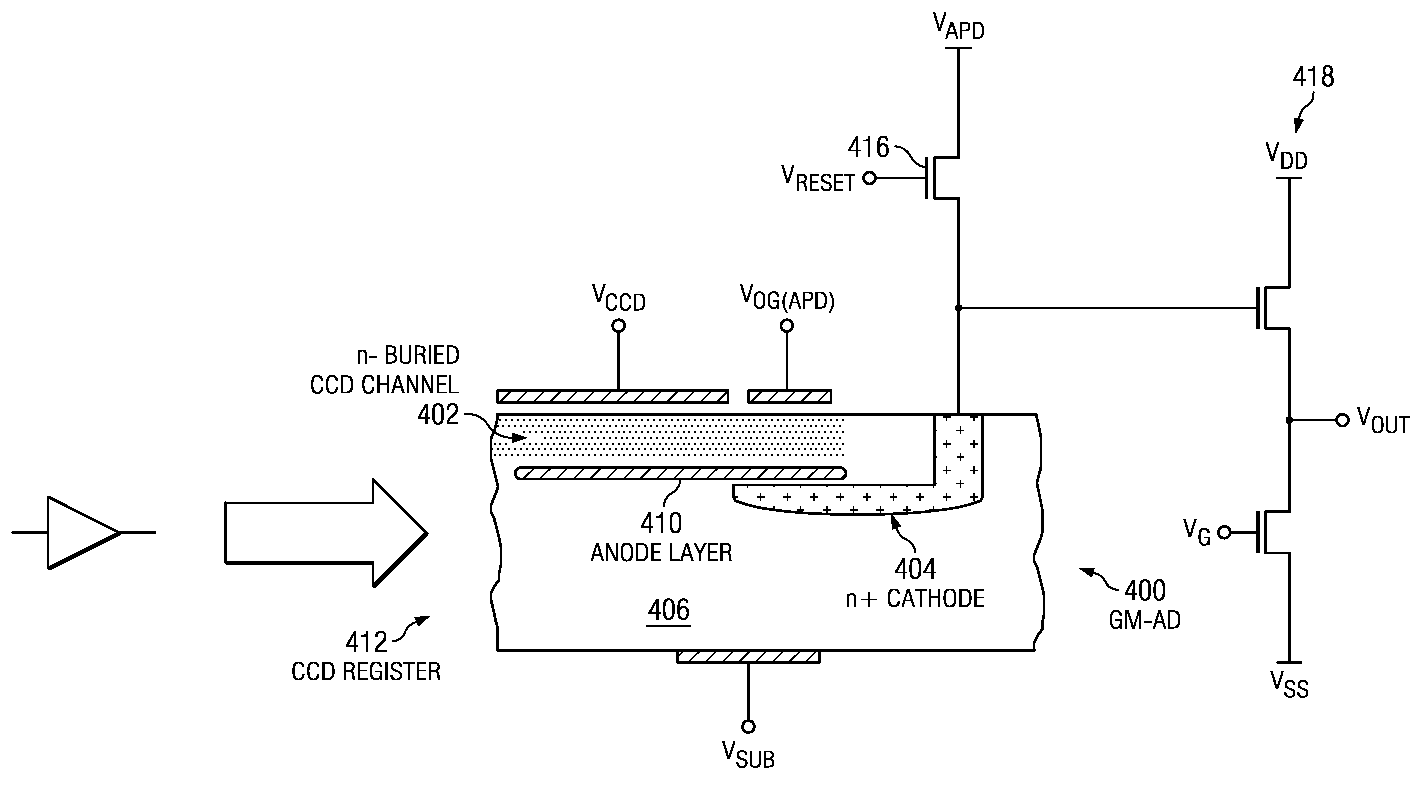
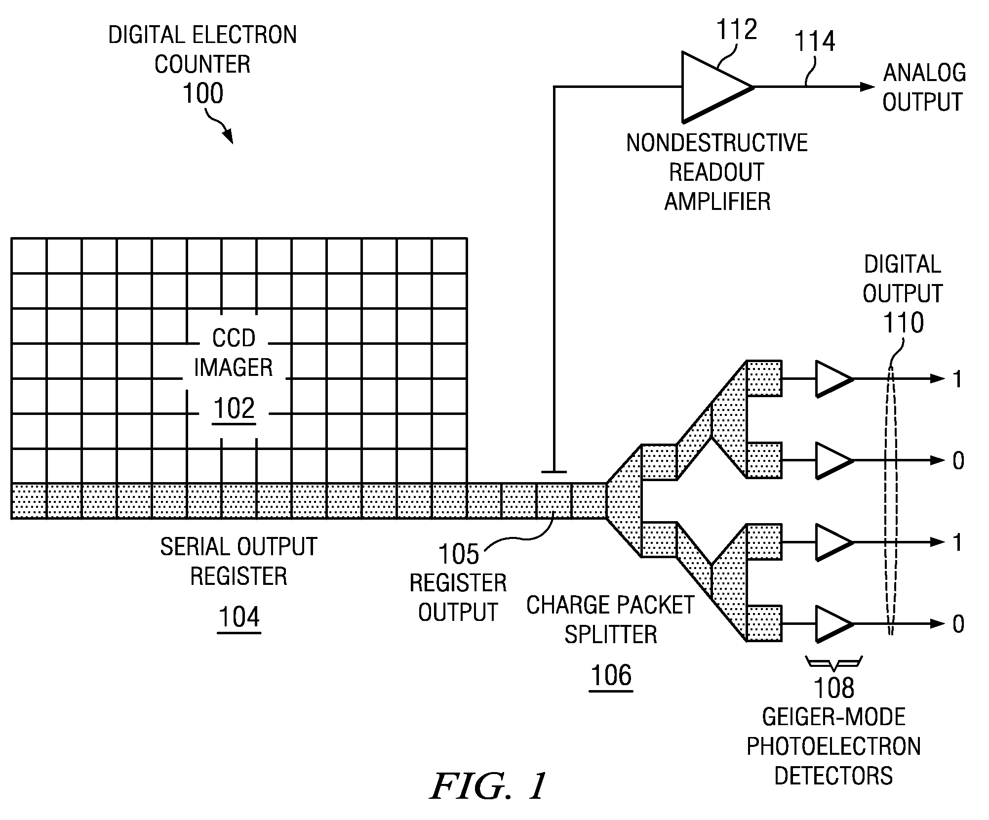
[0015]FIG. 1 is a block diagram of an electron counter 100 coupled to a CCD imager 102. The CCD imager 102 converts incident photons into photoelectrons whose spatial distribution follows the irradiance of the incident light. Each sensing element in the CCD imager 102 accumulates photoelectrons to form packets of charge that are transferred serially along the columns of the array to a serial output register 104 in the electron counter 100.

[0016]The serial output register 104, also known as a CCD register 104, transfers charge to a register output 105. A nondestructive readout amplifier 112 coupled to the register output 105 senses the transferred charge packet and generates an analog voltage 114 whose amplitude corresponds to the size of the charge packet. Generally, large charge packets produce voltages 114 whose amplitudes are well above the analog noise floor. If the charge packet is too small, however, then the amplitude of the analog voltage 114 may not be high enough above the...


PUM


Abstract

Embodiments of the present invention include an electron counter with a charge-coupled device (CCD) register configured to transfer electrons to a Geiger-mode avalanche diode (GM-AD) array operably coupled to the output of the CCD register. At high charge levels, a nondestructive amplifier senses the charge at the CCD register output to provide an analog indication of the charge. At low charge levels, noiseless charge splitters or meters divide the charge into single-electron packets, each of which is detected by a GM-AD that provides a digital output indicating whether an electron is present. Example electron counters are particularly well suited for counting photoelectrons generated by large-format, high-speed imaging arrays because they operate with high dynamic range and high sensitivity. As a result, they can be used to image scenes over a wide range of light levels.

Description

GOVERNMENT SUPPORT[0001]The invention was supported, in whole or in part, by grant FA8721-05-C-0002 from the Department of Defense and the Defense Advanced Research Projects Agency. The Government has certain rights in the invention.BACKGROUND OF THE INVENTION[0002]Many imaging applications require very sensitive light detection and wide dynamic range. An example is urban imaging where the light intensity can vary over several orders of magnitude (e.g., dark alleys to street lights). To achieve the best sensitivity, single photoelectron detection is needed, but often dynamic range is sacrificed. Several devices are available for detecting single photons (photoelectrons), such as photomultiplier tubes, intensified solid-state imagers, avalanche-register charge-coupled device (CCD) imagers, and Geiger-mode avalanche photodiodes. Each of these approaches has advantages for specific low-light-level imaging applications, but is limited in dynamic range.SUMMARY OF THE INVENTION[0003]Embod...

Claims


Application Information

Patent Timeline
Patent Type & Authority Applications(United States)
IPC IPC(8): H01L27/148H01L31/18H01L31/107
CPCH01L31/107H04N5/355H04N5/378H04N5/37213H01L31/18H04N5/357H04N25/57H04N25/60H04N25/713H04N25/75
Inventor SHAVER, DAVID C.KOSICKI, BERNARD B.REICH, ROBERT K.RATHMAN, DENNIS D.SCHUETTE, DANIEL R.AULL, BRIAN F.
Owner MASSACHUSETTS INST OF TECH
Why Eureka
Try Eureka