Methods and apparatus for applying periodic voltage using direct current

a technology of periodic voltage and power supply, applied in the field of plasma-based sputtering deposition, can solve the problems of complex operation, high construction and maintenance cost of high-frequency voltage source, and insufficient accuracy or otherwise satisfactory in many thin film processing applications

Active Publication Date: 2011-10-13
AES GLOBAL HLDG PTE LTD
View PDF2 Cites 57 Cited by
  • Summary
  • Abstract
  • Description
  • Claims
  • Application Information

AI Technical Summary

Benefits of technology

Other embodiments of the invention may be characterized as a power supply including a direct current power source configured to deliver power to a plasma sputtering chamber; a power control component in communication with the direct current power source and configured to direct the power to at least one electrode with an alternating polarity according to processor readable instructions; and a non-transitory, tangible computer readable storage medium, encoded with the processor readable instructions to perform a method for applying power, the method comprising: applying DC power pulses at a desired level of power to an electrode of a plasma processing chamber to sustain a plasma process that deposits a film on a substrate; monitoring an impedance of the plasma, the impedance providing an indication of a status of at least one processing effect; and adjusting, responsive to the monitored impedance, a frequency of the DC power pulses to alter the status of the processing effect.

Problems solved by technology

These high-frequency voltage sources are expensive to construct and maintain, as well as complicated to operate.
Although the present pulsed direct current power sources are functional, they are not sufficiently accurate or otherwise satisfactory in many thin film processing applications to achieve, for example, uniformity and / or particle generation thresholds.
Co-sputtering of an arbitrary stoichiometry is also not achievable with standard technology.

Method used


Image

  • Methods and apparatus for applying periodic voltage using direct current
  • Methods and apparatus for applying periodic voltage using direct current
  • Methods and apparatus for applying periodic voltage using direct current

Examples


Embodiment Construction

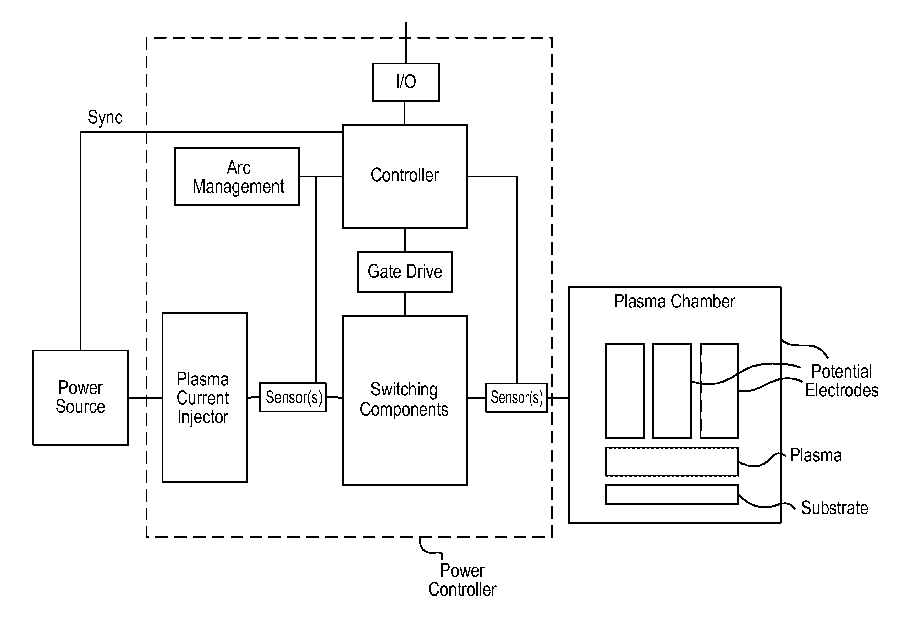
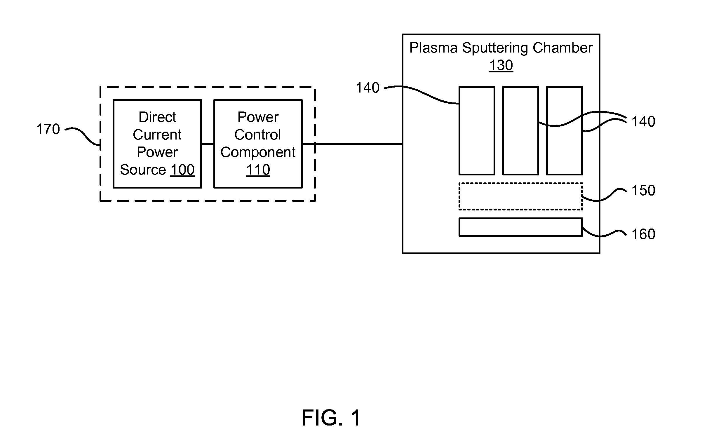
Referring now to the drawings, where like or similar elements are designated with identical reference numerals throughout the several views, and referring in particular to FIG. 1, it is a block diagram depicting a direct current (DC) power source 100, a power control component 110, and a plasma processing chamber 130, according to an embodiment of the invention. The plasma processing chamber 130 in the exemplary embodiment of FIG. 1 includes two or more electrodes 140 that are each configured to function as an anode and as a cathode (the cathode can be referred to as a sputtering target). The DC power source 100 and power control component 110 can be collectively referred to as a DC power supply 170. It should be recognized, however, that the block diagram of FIG. 1 is merely logical and in some embodiments the power source 100 and the power control component 110 are realized as separate components. In one embodiment for example, the power control component 110 is implemented as an ...


PUM

PropertyMeasurementUnit
poweraaaaaaaaaa
frequenciesaaaaaaaaaa

Abstract

Methods and apparatus for applying pulsed DC power to a plasma processing chamber are disclosed. In some implementations, frequency of the applied power is varied to achieve desired processing effects such as deposition rate, arc rate, and film characteristics. In addition, a method and apparatus are disclosed that utilize a relatively high potential during a reverse-potential portion of a particular cycle to mitigate possible nodule formation on the target. The relative durations of the reverse-potential portion, a sputtering portion, and a recovery portion of the cycle are adjustable to effectuate desired processing effects.

Description

FIELD OF THE INVENTIONThe present invention relates to plasma-based sputtering deposition. In particular, but not by way of limitation, the present invention relates to methods and apparatus for plasma-based processing using a direct current power supply.BACKGROUND OF THE INVENTIONPlasma processing techniques have found wide-spread use in industry for commercial processes such as plasma vapor deposition, sputtering, and so forth. These processes have become particularly useful in thin film applications. To generate plasma, a power supply creates an electric potential between a cathode and one or more anodes that are placed in a plasma chamber containing the process gases that form the plasma. When using these processes for deposition, the plasma acts upon the material of a target (also referred to as a sputtering source) placed in the plasma chamber that normally comprises the cathode surface. Plasma ions are accelerated towards the target and cause target material to be dislodged f...

Claims


Application Information

Patent Timeline
Patent Type & Authority Applications(United States)
IPC IPC(8): H05H1/48H05H1/00
CPCC23C14/3485C23C14/3492C23C14/54C23C14/542C23C14/548C23C14/564H05H2001/4682H01J37/3417H01J37/3429H01J37/3438H01J37/3444H01J37/3467H05H1/46H01J37/34H05H2242/22H01J37/32
Inventor NAUMAN, KENNETH E.FINLEY, KENNETHLARSON, SKIP B.PELLEYMOUNTER, DOUG
Owner AES GLOBAL HLDG PTE LTD
Why Eureka
Try Eureka